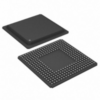
DS21FF42 Maxim Integrated Products, DS21FF42 Datasheet - Page 77

DS21FF42
Manufacturer Part Number
DS21FF42
Description
IC FRAMER T1 4X4 16CH 300-BGA
Manufacturer
Maxim Integrated Products
Datasheet
1.DS21FT42.pdf
(114 pages)
Specifications of DS21FF42
Controller Type
T1 Framer
Interface
Parallel/Serial
Voltage - Supply
2.97 V ~ 3.63 V
Current - Supply
300mA
Operating Temperature
0°C ~ 70°C
Mounting Type
Surface Mount
Package / Case
300-BGA
Lead Free Status / RoHS Status
Contains lead / RoHS non-compliant
Available stocks
Company
Part Number
Manufacturer
Quantity
Price
Company:
Part Number:
DS21FF42
Manufacturer:
LATTRON
Quantity:
9 020
The CCR2.0 bit should always be set to a one when the framer is inserting the FDL. More on how to use
the DS21Q42 in FDL applications is covered in a separate Application Note.
TFDL: TRANSMIT FDL REGISTER (Address = 7E Hex)
[Also used to insert Fs framing pattern in D4 framing mode; see Section 19.3]
The Transmit FDL Register (TFDL) contains the Facility Data Link (FDL) information that is to be
inserted on a byte basis into the outgoing T1 data stream. The LSB is transmitted first.
19.3 D4/SLC–96 OPERATION
In the D4 framing mode, the framer uses the TFDL register to insert the Fs framing pattern. To allow the
device to properly insert the Fs framing pattern, the TFDL register at address 7Eh must be programmed to
1Ch and the following bits must be programmed as shown: TCR1.2=0 (source Fs data from the TFDL
register) CCR2.5=1 (allow the TFDL register to load on multiframe boundaries)
Since the SLC–96 message fields share the Fs–bit position, the user can access the these message fields
via the TFDL and RFDL registers. Please see the separate Application Note for a detailed description of
how to implement a SLC–96
19.
Each framer in the DS21Q42 has the ability to generate and detect a repeating bit pattern that is from one
to eight bits in length. To transmit a pattern, the user will load the pattern to be sent into the Transmit
Code Definition (TCD) register and select the proper length of the pattern by setting the TC0 and TC1
bits in the In–Band Code Control (IBCC) register. Once this is accomplished, the pattern will be
transmitted as long as the TLOOP control bit (CCR3.1) is enabled. Normally (unless the transmit
formatter is programmed to not insert the F–bit position) the framer will overwrite the repeating pattern
once every 193 bits to allow the F–bit position to be sent. See Figure 24-15 for more details. As an
example, if the user wished to transmit the standard “loop up” code for Channel Service Units which is a
repeating pattern of ...10000100001... then 80h would be loaded into TDR and the length would set to 5
bits.
Each framer can detect two separate repeating patterns to allow for both a “loop up” code and a “loop
down” code to be detected. The user will program the codes to be detected in the Receive Up Code
Definition (RUPCD) register and the Receive Down Code Definition (RDNCD) register and the length of
each pattern will be selected via the IBCC register. The framer will detect repeating pattern codes in both
framed and unframed circumstances with bit error rates as high as 10**–2. The code detector has a
nominal integration period of 48 ms. Hence, after about 48 ms of receiving either code, the proper status
bit (LUP at SR1.7 and LDN at SR1.6) will be set to a one. Normally codes are sent for a period of 5
seconds. It is recommend that the software poll the framer every 100 ms to 1000 ms until 5 seconds has
elapsed to insure that the code is continuously present.
TFDL7
(MSB)
SYMBOL
TFDL7
TFDL0
PROGRAMMABLE IN–BAND CODE GENERATION AND DETECTION
TFDL6
POSITION
TFDL.7
TFDL.0
TFDL5
NAME AND DESCRIPTION
MSB of the FDL code to be transmitted
LSB of the FDL code to be transmitted
TFDL4
77 of 114
TFDL3
TFDL2
TFDL1
TFDL0
(LSB)


