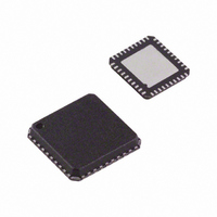
ADV7393BCPZ Analog Devices Inc, ADV7393BCPZ Datasheet - Page 29

ADV7393BCPZ
Manufacturer Part Number
ADV7393BCPZ
Description
IC DAC VIDEO HDTV 10BIT 40LFCSP
Manufacturer
Analog Devices Inc
Type
Video Encoderr
Datasheet
1.ADV7393BCPZ.pdf
(108 pages)
Specifications of ADV7393BCPZ
Design Resources
Reconstruction Video Filter Using ADA4430-1 Amplifier After ADV7393 Video Encoder (CN0101)
Applications
Set-Top Boxes, Video Players, Displays
Voltage - Supply, Analog
2.6 V ~ 3.46 V
Voltage - Supply, Digital
1.71 V ~ 1.89 V
Mounting Type
Surface Mount
Package / Case
40-LFCSP
Input Format
Digital
Output Format
Analog
Supply Voltage Range
1.71V To 1.89V
Operating Temperature Range
-40°C To +85°C
Tv / Video Case Style
LFCSP
No. Of Pins
40
Msl
MSL 1 - Unlimited
Lead Free Status / RoHS Status
Lead free / RoHS Compliant
For Use With
ADV7393-DBRDZ - BOARD EVAL FOR ADV7393EVAL-ADV7393EBZ - BOARD EVAL FOR ADV7393 ENCODER
Lead Free Status / RoHS Status
Lead free / RoHS Compliant, Lead free / RoHS Compliant
Available stocks
Company
Part Number
Manufacturer
Quantity
Price
Company:
Part Number:
ADV7393BCPZ
Manufacturer:
SIEMENS
Quantity:
101
Part Number:
ADV7393BCPZ
Manufacturer:
ADI/亚德诺
Quantity:
20 000
Company:
Part Number:
ADV7393BCPZ-3
Manufacturer:
ADI
Quantity:
302
Part Number:
ADV7393BCPZ-3
Manufacturer:
ADI/亚德诺
Quantity:
20 000
Company:
Part Number:
ADV7393BCPZ3
Manufacturer:
OSRAM
Quantity:
4 298
SR7 to
SR0
0x02
0x03
0x04
0x05
0x06
0x07
0x08
0x09
1
2
3
4
x = Logic 0 or Logic 1.
ED = enhanced definition = 525p and 625p.
Available on the ADV7392/ADV7393 (40-pin devices) only.
Subaddress 0x31, Bit 2 must also be enabled (ED/HD). Subaddress 0x84, Bit 6 must also be enabled (SD).
Register
Mode
Register 0
ED/HD
CSC
Matrix 0
ED/HD
CSC
Matrix 1
ED/HD
CSC
Matrix 2
ED/HD
CSC
Matrix 3
ED/HD
CSC
Matrix 4
ED/HD
CSC
Matrix 5
ED/HD
CSC
Matrix 6
Bit Description
Reserved
HD interlace external
and
Test pattern black bar
Manual CSC matrix adjust
Sync on RGB
RGB/YPrPb output select
SD sync output enable
ED/HD sync output enable
HSYNC
VSYNC
4
7
0
1
x
x
x
x
x
x
6
0
1
x
x
x
x
x
x
Rev. B | Page 29 of 108
5
0
1
x
x
x
x
x
x
Bit Number
4
0
1
x
x
x
x
x
x
3
0
1
x
x
x
x
x
x
1
2
0
1
x
x
x
x
x
x
ADV7390/ADV7391/ADV7392/ADV7393
1
0
1
x
x
x
x
x
x
x
0
0
x
x
x
x
x
x
x
Register Setting
LSBs for GV.
Bits[9:2] for GY.
Bits[9:2] for GU.
Bits[9:2] for GV.
Bits[9:2] for BU.
Bits[9:2] for RV.
Zero must be written to this bit.
Default.
If using HD
setting this bit to 1 is recommended (see the
HD Interlace External HSYNC and VSYNC
Considerations section for more information).
Disabled.
Enabled.
Disable manual CSC matrix adjust.
Enable manual CSC matrix adjust.
No sync.
Sync on all RGB outputs.
RGB component outputs.
YPrPb component outputs.
No sync output.
Output SD syncs on HSYNC and VSYNC pins.
No sync output.
Output ED/HD syncs on HSYNC and
VSYNC pins.
LSBs for GY.
LSBs for RV.
LSBs for BU.
LSBs for GU.
HSYNC
/
VSYNC
interlace mode,
Reset
Value
0x20
0x03
0xF0
0x4E
0x0E
0x24
0x92
0x7C


