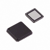
ADV7393BCPZ Analog Devices Inc, ADV7393BCPZ Datasheet - Page 69

ADV7393BCPZ
Manufacturer Part Number
ADV7393BCPZ
Description
IC DAC VIDEO HDTV 10BIT 40LFCSP
Manufacturer
Analog Devices Inc
Type
Video Encoderr
Datasheet
1.ADV7393BCPZ.pdf
(108 pages)
Specifications of ADV7393BCPZ
Design Resources
Reconstruction Video Filter Using ADA4430-1 Amplifier After ADV7393 Video Encoder (CN0101)
Applications
Set-Top Boxes, Video Players, Displays
Voltage - Supply, Analog
2.6 V ~ 3.46 V
Voltage - Supply, Digital
1.71 V ~ 1.89 V
Mounting Type
Surface Mount
Package / Case
40-LFCSP
Input Format
Digital
Output Format
Analog
Supply Voltage Range
1.71V To 1.89V
Operating Temperature Range
-40°C To +85°C
Tv / Video Case Style
LFCSP
No. Of Pins
40
Msl
MSL 1 - Unlimited
Lead Free Status / RoHS Status
Lead free / RoHS Compliant
For Use With
ADV7393-DBRDZ - BOARD EVAL FOR ADV7393EVAL-ADV7393EBZ - BOARD EVAL FOR ADV7393 ENCODER
Lead Free Status / RoHS Status
Lead free / RoHS Compliant, Lead free / RoHS Compliant
Available stocks
Company
Part Number
Manufacturer
Quantity
Price
Company:
Part Number:
ADV7393BCPZ
Manufacturer:
SIEMENS
Quantity:
101
Part Number:
ADV7393BCPZ
Manufacturer:
ADI/亚德诺
Quantity:
20 000
Company:
Part Number:
ADV7393BCPZ-3
Manufacturer:
ADI
Quantity:
302
Part Number:
ADV7393BCPZ-3
Manufacturer:
ADI/亚德诺
Quantity:
20 000
Company:
Part Number:
ADV7393BCPZ3
Manufacturer:
OSRAM
Quantity:
4 298
PRINTED CIRCUIT BOARD LAYOUT AND DESIGN
UNUSED PINS
If the HSYNC and VSYNC pins are not used, they should be tied
to V
other unused digital inputs should be tied to ground. Unused
digital output pins should be left floating. DAC outputs can
either be left floating or connected to GND. Disabling these
outputs is recommended.
DAC CONFIGURATIONS
The ADV739x contains three DACs. All three DACs can be
configured to operate in full-drive mode. Full-drive mode is
defined as 34.7 mA full-scale current into a 37.5 Ω load, R
Full drive is the recommended mode of operation for the DACs.
Alternatively, all three DACs can be configured to operate in low-
drive mode. Low-drive mode is defined as 4.33 mA full-scale
current into a 300 Ω load, R
The ADV739x contains an R
the R
current and, therefore, the output voltage levels of DAC 1, DAC 2,
and DAC 3. For full-drive operation, R
510 Ω and RL must have a value of 37.5 Ω. For low-drive opera-
tion, R
of 300 Ω. The resistor connected to the R
1% tolerance.
The ADV739x contains a compensation pin, COMP. A 2.2 nF
compensation capacitor should be connected from the COMP
pin to V
VIDEO OUTPUT BUFFER AND OPTIONAL
OUTPUT FILTER
An output buffer is necessary on any DAC that operates in low-
drive mode (R
produces a range of op amps suitable for this application, for
example, the AD8061. For more information about line driver
buffering circuits, see the relevant op amp data sheet.
An optional reconstruction (anti-imaging) low-pass filter (LPF)
may be required on the ADV739x DAC outputs. The filter
specifications vary with the application. The use of 16× (SD),
8× (ED), or 4× (HD) oversampling can remove the requirement
for a reconstruction filter altogether.
For applications requiring an output buffer and reconstruction
filter, the
buffers should be considered.
DD_IO
SET
SET
pin and AGND is used to control the full-scale output
AA
through a pull-up resistor (10 kΩ or 4.7 kΩ). Any
ADA4430-1
must have a value of 4.12 kΩ, and R
.
SET
= 4.12 kΩ, R
and
ADA4411-3
L
SET
.
L
pin. A resistor connected between
= 300 Ω). Analog Devices
SET
integrated video filter
SET
must have a value of
pin should have a
L
must have a value
L
.
Rev. B | Page 69 of 108
Table 58. ADV739x Output Rates
Input Mode
(Subaddress 0x01,
Bits[6:4])
SD
ED
HD
Table 59. Output Filter Requirements
Application
SD
ED
HD
OUTPUT
OUTPUT
OUTPUT
DAC
DAC
DAC
ADV7390/ADV7391/ADV7392/ADV7393
300Ω
Figure 90. Example of Output Filter for SD, 16× Oversampling
Figure 92. Example of Output Filter for HD, 4× Oversampling
Figure 91. Example of Output Filter for ED, 8× Oversampling
600Ω
3
4
600Ω
10µH
22pF
Oversampling
2×
8×
16×
1×
4×
8×
1×
2×
4×
6.8pF
4.7µH
6.8pF
1
75Ω
Oversampling
Off
On
On
Off
On
On
Off
On
On
600Ω
390nH
33pF
600Ω
560Ω
560Ω
3
4
3
4
33pF
Cutoff
Frequency
(MHz)
> 6.5
> 6.5
> 6.5
> 12.5
> 12.5
> 12.5
> 30
> 30
> 30
560Ω
560Ω
75Ω
Output Rate (MHz)
27
108
216
27
108
216
74.25
148.5
297
1
1
500Ω
3
4
75Ω
75Ω
500Ω
Attenuation
–50 dB
(MHz)
20.5
101.5
209.5
14.5
95.5
203.5
44.25
118.5
267
(2×)
(8×)
(16×)
(1×)
(4×)
(8×)
(1×)
(2×)
(4×)
1
OUTPUT
BNC
OUTPUT
BNC
OUTPUT
BNC
at


