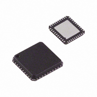
ADV7393BCPZ Analog Devices Inc, ADV7393BCPZ Datasheet - Page 9

ADV7393BCPZ
Manufacturer Part Number
ADV7393BCPZ
Description
IC DAC VIDEO HDTV 10BIT 40LFCSP
Manufacturer
Analog Devices Inc
Type
Video Encoderr
Datasheet
1.ADV7393BCPZ.pdf
(108 pages)
Specifications of ADV7393BCPZ
Design Resources
Reconstruction Video Filter Using ADA4430-1 Amplifier After ADV7393 Video Encoder (CN0101)
Applications
Set-Top Boxes, Video Players, Displays
Voltage - Supply, Analog
2.6 V ~ 3.46 V
Voltage - Supply, Digital
1.71 V ~ 1.89 V
Mounting Type
Surface Mount
Package / Case
40-LFCSP
Input Format
Digital
Output Format
Analog
Supply Voltage Range
1.71V To 1.89V
Operating Temperature Range
-40°C To +85°C
Tv / Video Case Style
LFCSP
No. Of Pins
40
Msl
MSL 1 - Unlimited
Lead Free Status / RoHS Status
Lead free / RoHS Compliant
For Use With
ADV7393-DBRDZ - BOARD EVAL FOR ADV7393EVAL-ADV7393EBZ - BOARD EVAL FOR ADV7393 ENCODER
Lead Free Status / RoHS Status
Lead free / RoHS Compliant, Lead free / RoHS Compliant
Available stocks
Company
Part Number
Manufacturer
Quantity
Price
Company:
Part Number:
ADV7393BCPZ
Manufacturer:
SIEMENS
Quantity:
101
Part Number:
ADV7393BCPZ
Manufacturer:
ADI/亚德诺
Quantity:
20 000
Company:
Part Number:
ADV7393BCPZ-3
Manufacturer:
ADI
Quantity:
302
Part Number:
ADV7393BCPZ-3
Manufacturer:
ADI/亚德诺
Quantity:
20 000
Company:
Part Number:
ADV7393BCPZ3
Manufacturer:
OSRAM
Quantity:
4 298
DIGITAL TIMING SPECIFICATIONS—3.3 V
V
All specifications T
Table 9.
Parameter
VIDEO DATA AND VIDEO CONTROL PORT
PIPELINE DELAY
RESET CONTROL
1
2
3
4
5
SD = standard definition, ED = enhanced definition (525p/625p), HD = high definition, SDR = single data rate, DDR = dual data rate.
Video data: P[15:0] for ADV7392/ADV7393 or P[7:0] for ADV7390/ADV7391.
Video control: HSYNC and VSYNC .
Guaranteed by characterization.
Guaranteed by design.
DD
Data Input Setup Time, t
Data Input Hold Time, t
Control Input Setup Time, t
Control Input Hold Time, t
Control Output Access Time, t
Control Output Hold Time, t
SD
ED
HD
RESET Low Time
= 1.71 V to 1.89 V, PV
CVBS/Y-C Outputs (2×)
CVBS/Y-C Outputs (8×)
CVBS/Y-C Outputs (16×)
Component Outputs (2×)
Component Outputs (8×)
Component Outputs (16×)
Component Outputs (1×)
Component Outputs (4×)
Component Outputs (8×)
Component Outputs (1×)
Component Outputs (2×)
Component Outputs (4×)
1
1
1
5
MIN
to T
12
11
DD
4
MAX
4
12
11
= 1.71 V to 1.89 V, V
4
14
4
(−40°C to +85°C), unless otherwise noted.
4
13
4
2, 3
AA
Conditions
SD
ED/HD-SDR
ED/HD-DDR
ED (at 54 MHz)
SD
ED/HD-SDR
ED/HD-DDR
ED (at 54 MHz)
SD
ED/HD-SDR or ED/HD-DDR
ED (at 54 MHz)
SD
ED/HD-SDR or ED/HD-DDR
ED (at 54 MHz)
SD
ED/HD-SDR, ED/HD-DDR, or ED (at 54 MHz)
SD
ED/HD-SDR, ED/HD-DDR, or ED (at 54 MHz)
SD oversampling disabled
SD oversampling enabled
SD oversampling enabled
SD oversampling disabled
SD oversampling enabled
SD oversampling enabled
ED oversampling disabled
ED oversampling enabled
ED oversampling enabled
HD oversampling disabled
HD oversampling enabled
HD oversampling enabled
= 2.6 V to 3.465 V, V
Rev. B | Page 9 of 108
1
DD_IO
ADV7390/ADV7391/ADV7392/ADV7393
= 2.97 V to 3.63 V.
Min
2.1
2.3
2.3
1.7
1.0
1.1
1.1
1.0
2.1
2.3
1.7
1.0
1.1
1.0
4.0
3.5
100
Typ
68
79
67
78
69
41
40
42
84
49
46
44
Max
12
10
Unit
ns
ns
ns
ns
ns
ns
ns
ns
ns
ns
ns
ns
ns
ns
Clock cycles
Clock cycles
Clock cycles
Clock cycles
Clock cycles
Clock cycles
Clock cycles
Clock cycles
Clock cycles
Clock cycles
Clock cycles
Clock cycles
ns
ns
ns
ns
ns


