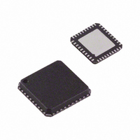
ADV7393BCPZ Analog Devices Inc, ADV7393BCPZ Datasheet - Page 67

ADV7393BCPZ
Manufacturer Part Number
ADV7393BCPZ
Description
IC DAC VIDEO HDTV 10BIT 40LFCSP
Manufacturer
Analog Devices Inc
Type
Video Encoderr
Datasheet
1.ADV7393BCPZ.pdf
(108 pages)
Specifications of ADV7393BCPZ
Design Resources
Reconstruction Video Filter Using ADA4430-1 Amplifier After ADV7393 Video Encoder (CN0101)
Applications
Set-Top Boxes, Video Players, Displays
Voltage - Supply, Analog
2.6 V ~ 3.46 V
Voltage - Supply, Digital
1.71 V ~ 1.89 V
Mounting Type
Surface Mount
Package / Case
40-LFCSP
Input Format
Digital
Output Format
Analog
Supply Voltage Range
1.71V To 1.89V
Operating Temperature Range
-40°C To +85°C
Tv / Video Case Style
LFCSP
No. Of Pins
40
Msl
MSL 1 - Unlimited
Lead Free Status / RoHS Status
Lead free / RoHS Compliant
For Use With
ADV7393-DBRDZ - BOARD EVAL FOR ADV7393EVAL-ADV7393EBZ - BOARD EVAL FOR ADV7393 ENCODER
Lead Free Status / RoHS Status
Lead free / RoHS Compliant, Lead free / RoHS Compliant
Available stocks
Company
Part Number
Manufacturer
Quantity
Price
Company:
Part Number:
ADV7393BCPZ
Manufacturer:
SIEMENS
Quantity:
101
Part Number:
ADV7393BCPZ
Manufacturer:
ADI/亚德诺
Quantity:
20 000
Company:
Part Number:
ADV7393BCPZ-3
Manufacturer:
ADI
Quantity:
302
Part Number:
ADV7393BCPZ-3
Manufacturer:
ADI/亚德诺
Quantity:
20 000
Company:
Part Number:
ADV7393BCPZ3
Manufacturer:
OSRAM
Quantity:
4 298
PIXEL AND CONTROL PORT READBACK
Subaddress 0x13, Subaddress 0x14, Subaddress 0x16
The ADV739x supports the readback of most digital inputs via
the I
connectivity testing with upstream devices.
The pixel port (P[15:0] or P[7:0]), HSYNC , VSYNC , and SFL
are available for readback via the MPU port. The readback
registers are located at Subaddress 0x13, Subaddress 0x14, and
Subaddress 0x16.
When using this feature, apply a clock signal to the CLKIN pin
to register the levels applied to the input pins. The SD input
mode (Subaddress 0x01, Bits[6:4] = 000) must be selected when
using this feature.
RESET MECHANISMS
Subaddress 0x17, Bit 1
A hardware reset is activated with a high-to-low transition on
the RESET pin in accordance with the timing specifications.
This resets all registers to their default values. After a hardware
reset, the MPU port is configured for I
device operation, a hardware reset is necessary after power-up.
The ADV739x also has a software reset accessible via the I
MPU port. A software reset is activated by writing a 1 to
Subaddress 0x17, Bit 1. This resets all registers to their default
values. This bit is self-clearing; that is, after a 1 has been written
to the bit, the bit automatically returns to 0.
A hardware reset is necessary after power-up for correct device
operation. If no hardware reset functionality is required by the
application, the RESET pin can be connected to an RC network
to provide the hardware reset necessary after power-up. After
power-up, the time constant of the RC network holds the
2
C MPU port. This feature is useful for board-level
TELETEXT VBI LINE
2
C operation. For correct
Figure 88. Teletext VBI Line
2
C
Rev. B | Page 67 of 108
RUN-IN CLOCK
45 BYTES (360 BITS) – PAL
ADDRESS AND DATA
RESET pin low long enough to cause a reset to take place. All
subsequent resets can be done via software.
SD TELETEXT INSERTION
Subaddress 0xC9 to Subaddress 0xCE
The ADV739x supports the insertion of teletext data, using a
two pin interface, when operating in PAL mode. Teletext
insertion is enabled using Subaddress 0xC9, Bit 0.
In accordance with the PAL WST teletext standard, teletext data
should be inserted into the ADV739x at a rate of 6.9375 Mbps.
On the ADV7390/ADV7391, the teletext data is inserted on the
VSYNC pin. On the ADV7392/ADV7393, the teletext data can
be inserted on the VSYNC or P0 pin (selectable through
Subaddress 0xC9, Bit 2).
When teletext insertion is enabled, a teletext request signal is
output from the ADV739x to indicate when teletext data should
be inserted. The teletext request signal is output on the SFL pin.
The position (relative to the teletext data) and width of the
request signal are configurable using Subaddress 0xCA. The
request signal can operate in either a line or bit mode. The
request signal mode is controlled using Subaddress 0xC9, Bit 1.
To account for the noninteger relationship between the teletext
insertion rate (6.9375 Mbps) and the pixel clock (27 MHz), a
teletext insertion protocol is implemented in the ADV739x. At a
rate of 6.9375 Mbps, the time taken for the insertion of 37
teletext bits equates to 144 pixel clock cycles (at 27 MHz). For
every 37 teletext bits inserted into the ADV739x, the 10
28
remainder are carried for four pixel clock cycles (totaling 144
pixel clock cycles). The teletext insertion protocol repeats every
37 teletext bits or 144 pixel clock cycles until all 360 teletext bits
are inserted.
th
ADV7390/ADV7391/ADV7392/ADV7393
, and 37
th
bits are carried for three pixel clock cycles, and the
th
, 19
th
,


