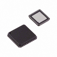
ADV7393BCPZ Analog Devices Inc, ADV7393BCPZ Datasheet - Page 70

ADV7393BCPZ
Manufacturer Part Number
ADV7393BCPZ
Description
IC DAC VIDEO HDTV 10BIT 40LFCSP
Manufacturer
Analog Devices Inc
Type
Video Encoderr
Datasheet
1.ADV7393BCPZ.pdf
(108 pages)
Specifications of ADV7393BCPZ
Design Resources
Reconstruction Video Filter Using ADA4430-1 Amplifier After ADV7393 Video Encoder (CN0101)
Applications
Set-Top Boxes, Video Players, Displays
Voltage - Supply, Analog
2.6 V ~ 3.46 V
Voltage - Supply, Digital
1.71 V ~ 1.89 V
Mounting Type
Surface Mount
Package / Case
40-LFCSP
Input Format
Digital
Output Format
Analog
Supply Voltage Range
1.71V To 1.89V
Operating Temperature Range
-40°C To +85°C
Tv / Video Case Style
LFCSP
No. Of Pins
40
Msl
MSL 1 - Unlimited
Lead Free Status / RoHS Status
Lead free / RoHS Compliant
For Use With
ADV7393-DBRDZ - BOARD EVAL FOR ADV7393EVAL-ADV7393EBZ - BOARD EVAL FOR ADV7393 ENCODER
Lead Free Status / RoHS Status
Lead free / RoHS Compliant, Lead free / RoHS Compliant
Available stocks
Company
Part Number
Manufacturer
Quantity
Price
Company:
Part Number:
ADV7393BCPZ
Manufacturer:
SIEMENS
Quantity:
101
Part Number:
ADV7393BCPZ
Manufacturer:
ADI/亚德诺
Quantity:
20 000
Company:
Part Number:
ADV7393BCPZ-3
Manufacturer:
ADI
Quantity:
302
Part Number:
ADV7393BCPZ-3
Manufacturer:
ADI/亚德诺
Quantity:
20 000
Company:
Part Number:
ADV7393BCPZ3
Manufacturer:
OSRAM
Quantity:
4 298
ADV7390/ADV7391/ADV7392/ADV7393
–10
–20
–30
–40
–50
–60
–70
–80
–90
–10
–20
–30
–40
–50
–60
–70
–80
–10
–20
–30
–40
–50
0
1M
0
1M
0
1
GROUP DELAY (Seconds)
GROUP DELAY (Seconds)
Figure 93. Output Filter Plot for SD, 16× Oversampling
Figure 95. Output Filter Plot for HD, 4× Oversampling
Figure 94. Output Filter Plot for ED, 8× Oversampling
GROUP DELAY (Seconds)
CIRCUIT FREQUENCY RESPONSE
CIRCUIT FREQUENCY RESPONSE
CIRCUIT FREQUENCY RESPONSE
10M
10M
FREQUENCY (Hz)
FREQUENCY (MHz)
FREQUENCY (Hz)
10
MAGNITUDE (dB)
100M
100M
MAGNITUDE (dB)
MAGNITUDE (dB)
PHASE (Degrees)
100
(Degrees)
PHASE
(Degrees)
PHASE
1G
1G
480
400
320
240
160
80
0
–80
–160
–240
0
–30
–60
–90
–120
–150
–180
–210
–240
200
120
40
–40
–120
–200
18n
16n
14n
12n
10n
8n
6n
4n
2n
0
24n
21n
18n
15n
12n
9n
6n
3n
0
Rev. B | Page 70 of 108
PRINTED CIRCUIT BOARD (PCB) LAYOUT
The ADV739x is a highly integrated circuit containing both
precision analog and high speed digital circuitry. It is designed
to minimize interference effects on the integrity of the analog
circuitry by the high speed digital circuitry. It is imperative that
these same design and layout techniques be applied to the
system-level design so that optimal performance is achieved.
The layout should be optimized for lowest noise on the
ADV739x power and ground planes by shielding the digital
inputs and providing good power supply decoupling.
It is recommended to use a 4-layer printed circuit board with
ground and power planes separating the signal trace layer and
the solder side layer.
Component Placement
Component placement should be carefully considered to
separate noisy circuits, such as clock signals and high speed
digital circuitry, from analog circuitry.
The external loop filter components and components connected
to the COMP and R
to, and on the same side of the PCB as, the ADV739x. Adding
vias to the PCB to get the components closer to the ADV739x is
not recommended.
It is recommended that the ADV739x be placed as close as
possible to the output connector, with the DAC output traces as
short as possible.
The termination resistors on the DAC output traces should be
placed as close as possible to and on the same side of the PCB as
the ADV739x. The termination resistors should overlay the
PCB ground plane.
External filter and buffer components connected to the DAC
outputs should be placed as close as possible to the ADV739x to
minimize the possibility of noise pickup from neighboring
circuitry and to minimize the effect of trace capacitance on
output bandwidth. This is particularly important when
operating in low-drive mode (R
Power Supplies
It is recommended that a separate regulated supply be provided
for each power domain (V
optimal performance, linear regulators rather than switch mode
regulators should be used. If switch mode regulators must be
used, care must be taken with regard to the quality of the output
voltage in terms of ripple and noise. This is particularly true for
the V
individually connected to the system power supply at a single
point through a suitable filtering device, such as a ferrite bead.
AA
and PV
DD
power domains. Each power supply should be
SET
pins should be placed as close as possible
AA
, V
DD
SET
, V
= 4.12 kΩ, R
DD_IO
, and PV
L
= 300 Ω).
DD
). For


