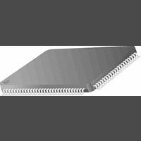
PC87393VJG National Semiconductor, PC87393VJG Datasheet - Page 109

PC87393VJG
Manufacturer Part Number
PC87393VJG
Description
IC, SUPER I/O DEVICE, TQFP-100
Manufacturer
National Semiconductor
Specifications of PC87393VJG
Data Rate
2Mbps
Supply Voltage Range
3V to 3.6V
Logic Case Style
TQFP
No. Of Pins
100
Operating Temperature Range
0°C to +70°C
Termination Type
SMD
Transceiver Type
Interface
Rohs Compliant
No
Available stocks
Company
Part Number
Manufacturer
Quantity
Price
Part Number:
PC87393VJG
Manufacturer:
NS/国半
Quantity:
20 000
- Current page: 109 of 148
- Download datasheet (2Mb)
7.0 X-Bus Extension
Once a write cycle on the LPC falls within the range of any of the enabled decoded address ranges of the X-Bus functional
block, a write cycle begins. A write cycle (Figure 25) starts by outputting the address signals on address signals XA19-0,
and the data signals on data pins XD7-0, on the rising edge of the clock. One LPC clock cycle later, a chip select signals
XCS1 or 0 is asserted, based on the address accessed and the select signal mapping. Three clock cycles later, on the next
rising edge of the clock, the XWR signal is asserted (set to 0) indicating that this is a write cycle and enabling the device to
be written for 16 clock cycles plus the internally programmed wait state period. If XRDY use is enabled for this zone, XRDY
input value is then checked on the rising edge of the clock, and the transaction is extended until XRDY is detected to be high.
Five LPC clock cycles later, XWR is de-asserted (set to 1) and one clock cycle later, the transaction is completed by de-
asserting XCS1-0. Two clock cycle later, the address lines change their values to 0.
(Data Read)
CLK
(Internal for
Reference)
XD7-0
XA19-0
XCS1-0
XWR
XRD
XRDY
(Continued)
Figure 24. Read Access Cycle - Normal Address Mode
Insert 12+”Programmed Wait States” of 33 MHz clocks here.
All non-clock signals remain the same during this inserted time.
109
XD[7:0] (Data In)
www.national.com
Related parts for PC87393VJG
Image
Part Number
Description
Manufacturer
Datasheet
Request
R
Part Number:
Description:
National Semiconductor [8-Bit D/A Converter]
Manufacturer:
National Semiconductor
Datasheet:
Part Number:
Description:
National Semiconductor [Media Coprocessor]
Manufacturer:
National Semiconductor
Datasheet:
Part Number:
Description:
Digitally Controlled Tone and Volume Circuit with Stereo Audio Power Amplifier, Microphone Preamp Stage and National 3D Sound
Manufacturer:
National Semiconductor
Datasheet:
Part Number:
Description:
Digitally Controlled Tone and Volume Circuit with Stereo Audio Power Amplifier, Microphone Preamp Stage and National 3D Sound
Manufacturer:
National Semiconductor
Datasheet:
Part Number:
Description:
AC97 Rev 2 Codec with Sample Rate Conversion and National 3D Sound
Manufacturer:
National Semiconductor
Part Number:
Description:
Manufacturer:
National Semiconductor
Datasheet:
Part Number:
Description:
Manufacturer:
National Semiconductor
Datasheet:
Part Number:
Description:
General Purpose, Low Voltage, Low Power, Rail-to-Rail Output Operational Amplifiers
Manufacturer:
National Semiconductor
Datasheet:
Part Number:
Description:
8-bit 20 MSPS flash A/D converter.
Manufacturer:
National Semiconductor
Datasheet:
Part Number:
Description:
Low Noise Quad Operational Amplifier
Manufacturer:
National Semiconductor
Datasheet:
Part Number:
Description:
Quad Differential Line Receivers
Manufacturer:
National Semiconductor
Datasheet:
Part Number:
Description:
Quad High Speed Trapezoidal? Bus Transceiver
Manufacturer:
National Semiconductor
Datasheet:
Part Number:
Description:
Dual Line Receiver
Manufacturer:
National Semiconductor
Datasheet:
Part Number:
Description:
TTL to 10k ECL Level Translator with Latch
Manufacturer:
National Semiconductor
Datasheet:


