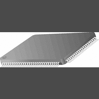
PC87393VJG National Semiconductor, PC87393VJG Datasheet - Page 140

PC87393VJG
Manufacturer Part Number
PC87393VJG
Description
IC, SUPER I/O DEVICE, TQFP-100
Manufacturer
National Semiconductor
Specifications of PC87393VJG
Data Rate
2Mbps
Supply Voltage Range
3V to 3.6V
Logic Case Style
TQFP
No. Of Pins
100
Operating Temperature Range
0°C to +70°C
Termination Type
SMD
Transceiver Type
Interface
Rohs Compliant
No
Available stocks
Company
Part Number
Manufacturer
Quantity
Price
Part Number:
PC87393VJG
Manufacturer:
NS/国半
Quantity:
20 000
- Current page: 140 of 148
- Download datasheet (2Mb)
www.national.com
9.0 Device Characteristics
9.4.3
3.3 V Clock
LCLK and LRESET
0.3 V
0.4 V
DD
0.5 V
DD
Symbol
t
t
t
CYC
HIGH
DD
LOW
1. The PCI may have any clock frequency between nominal DC and 33
2. Rise and fall times are specified in terms of the edge rate measured in
3. The minimum LRESET slew rate applies only to the rising (de-assertion)
-
-
1
LCLK Cycle Time
LCLK High Time
LCLK Low Time
LCLK Slew Rate
LRESET Slew Rate
MHz. Device operational parameters at frequencies under 16 MHz
may be guaranteed by design rather than by testing. The clock fre-
quency may be changed at any time during the operation of the sys-
tem as long as the clock edges remain “clean” (monotonic) and the
minimum cycle and high and low times are not violated. The clock
may only be stopped in a low state.
V/ns. This slew rate must be met across the minimum peak-to-peak
portion of the clock wavering as shown below.
edge of the reset signal, and ensures that system noise cannot ren-
der an otherwise a monotonic signal to appear to bounce in the
switching range.
0.6 V
(Continued)
t
HIGH
DD
Parameter
2
3
t
CYC
140
0.2 V
t
LOW
DD
Min
30
11
11
50
1
Max
4
mV/ns
Units
V/ns
0.4 V
(minimum)
ns
ns
ns
DD
p-to-p
Related parts for PC87393VJG
Image
Part Number
Description
Manufacturer
Datasheet
Request
R
Part Number:
Description:
National Semiconductor [8-Bit D/A Converter]
Manufacturer:
National Semiconductor
Datasheet:
Part Number:
Description:
National Semiconductor [Media Coprocessor]
Manufacturer:
National Semiconductor
Datasheet:
Part Number:
Description:
Digitally Controlled Tone and Volume Circuit with Stereo Audio Power Amplifier, Microphone Preamp Stage and National 3D Sound
Manufacturer:
National Semiconductor
Datasheet:
Part Number:
Description:
Digitally Controlled Tone and Volume Circuit with Stereo Audio Power Amplifier, Microphone Preamp Stage and National 3D Sound
Manufacturer:
National Semiconductor
Datasheet:
Part Number:
Description:
AC97 Rev 2 Codec with Sample Rate Conversion and National 3D Sound
Manufacturer:
National Semiconductor
Part Number:
Description:
Manufacturer:
National Semiconductor
Datasheet:
Part Number:
Description:
Manufacturer:
National Semiconductor
Datasheet:
Part Number:
Description:
General Purpose, Low Voltage, Low Power, Rail-to-Rail Output Operational Amplifiers
Manufacturer:
National Semiconductor
Datasheet:
Part Number:
Description:
8-bit 20 MSPS flash A/D converter.
Manufacturer:
National Semiconductor
Datasheet:
Part Number:
Description:
Low Noise Quad Operational Amplifier
Manufacturer:
National Semiconductor
Datasheet:
Part Number:
Description:
Quad Differential Line Receivers
Manufacturer:
National Semiconductor
Datasheet:
Part Number:
Description:
Quad High Speed Trapezoidal? Bus Transceiver
Manufacturer:
National Semiconductor
Datasheet:
Part Number:
Description:
Dual Line Receiver
Manufacturer:
National Semiconductor
Datasheet:
Part Number:
Description:
TTL to 10k ECL Level Translator with Latch
Manufacturer:
National Semiconductor
Datasheet:


