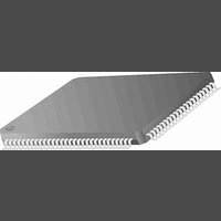
PC87393VJG National Semiconductor, PC87393VJG Datasheet - Page 127

PC87393VJG
Manufacturer Part Number
PC87393VJG
Description
IC, SUPER I/O DEVICE, TQFP-100
Manufacturer
National Semiconductor
Specifications of PC87393VJG
Data Rate
2Mbps
Supply Voltage Range
3V to 3.6V
Logic Case Style
TQFP
No. Of Pins
100
Operating Temperature Range
0°C to +70°C
Termination Type
SMD
Transceiver Type
Interface
Rohs Compliant
No
Available stocks
Company
Part Number
Manufacturer
Quantity
Price
Part Number:
PC87393VJG
Manufacturer:
NS/国半
Quantity:
20 000
- Current page: 127 of 148
- Download datasheet (2Mb)
8.0 Legacy Functional Blocks
8.3.3
SP1 and SP2 Register Maps for UART Functionality
04h - 07h
Offset
Offset
00h
00h
01h
02h
03h
04h
05h
06h
07h
00h
01h
02h
03h
1. When bit 7 of this Register is set to 1, bits 6-0 of BSR select the bank, as
SPR/ASCR Scratchpad/Auxiliary Status and Control
shown in Table 38.
Mnemonic
Mnemonic
LCR/BSR Line Control/Bank Select
LBGD(H)
LBGD(L)
7
0
1
1
1
1
1
1
1
1
1
BSR
LCR
MCR
MSR
RXD
FCR
TXD
LSR
IER
EIR
6
0
1
1
1
1
1
1
1
1
x
1
1
5
1
1
1
1
1
1
x
x
x
x
Table 38. Bank Selection Encoding
BSR Bits
(Continued)
Receiver Data Port
Transmitter Data Port
Interrupt Enable
Event Identification (Read Cycles)
FIFO Control (Write Cycles)
Line Control
Bank Select
Modem/Mode Control
Link Status
Modem Status
Legacy Baud Generator Divisor Port (Low Byte)
Legacy Baud Generator Divisor Port (High Byte)
4
0
0
0
0
1
1
Table 37. Bank 0 Register Map
x
x
x
x
Table 39. Bank 1 Register Map
3
x
x
x
x
0
0
1
1
0
0
2
x
x
x
x
0
1
0
1
0
1
1
x
x
1
x
0
0
0
0
0
0
127
Register Name
Register Name
0
x
x
x
1
0
0
0
0
0
0
Reserved
Reserved
Selected
Bank
0
1
1
1
2
3
4
5
6
7
(SP1 + SP2)
Functionality
UART + IR
IR Only
(SP2)
Type
Type
R/W
R/W
R/W
R/W
R/W
R/W
R/W
RO
RO
RO
RO
W
W
www.national.com
Related parts for PC87393VJG
Image
Part Number
Description
Manufacturer
Datasheet
Request
R
Part Number:
Description:
National Semiconductor [8-Bit D/A Converter]
Manufacturer:
National Semiconductor
Datasheet:
Part Number:
Description:
National Semiconductor [Media Coprocessor]
Manufacturer:
National Semiconductor
Datasheet:
Part Number:
Description:
Digitally Controlled Tone and Volume Circuit with Stereo Audio Power Amplifier, Microphone Preamp Stage and National 3D Sound
Manufacturer:
National Semiconductor
Datasheet:
Part Number:
Description:
Digitally Controlled Tone and Volume Circuit with Stereo Audio Power Amplifier, Microphone Preamp Stage and National 3D Sound
Manufacturer:
National Semiconductor
Datasheet:
Part Number:
Description:
AC97 Rev 2 Codec with Sample Rate Conversion and National 3D Sound
Manufacturer:
National Semiconductor
Part Number:
Description:
Manufacturer:
National Semiconductor
Datasheet:
Part Number:
Description:
Manufacturer:
National Semiconductor
Datasheet:
Part Number:
Description:
General Purpose, Low Voltage, Low Power, Rail-to-Rail Output Operational Amplifiers
Manufacturer:
National Semiconductor
Datasheet:
Part Number:
Description:
8-bit 20 MSPS flash A/D converter.
Manufacturer:
National Semiconductor
Datasheet:
Part Number:
Description:
Low Noise Quad Operational Amplifier
Manufacturer:
National Semiconductor
Datasheet:
Part Number:
Description:
Quad Differential Line Receivers
Manufacturer:
National Semiconductor
Datasheet:
Part Number:
Description:
Quad High Speed Trapezoidal? Bus Transceiver
Manufacturer:
National Semiconductor
Datasheet:
Part Number:
Description:
Dual Line Receiver
Manufacturer:
National Semiconductor
Datasheet:
Part Number:
Description:
TTL to 10k ECL Level Translator with Latch
Manufacturer:
National Semiconductor
Datasheet:


