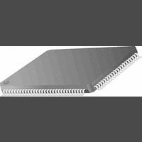
PC87393VJG National Semiconductor, PC87393VJG Datasheet - Page 87

PC87393VJG
Manufacturer Part Number
PC87393VJG
Description
IC, SUPER I/O DEVICE, TQFP-100
Manufacturer
National Semiconductor
Specifications of PC87393VJG
Data Rate
2Mbps
Supply Voltage Range
3V to 3.6V
Logic Case Style
TQFP
No. Of Pins
100
Operating Temperature Range
0°C to +70°C
Termination Type
SMD
Transceiver Type
Interface
Rohs Compliant
No
Available stocks
Company
Part Number
Manufacturer
Quantity
Price
Part Number:
PC87393VJG
Manufacturer:
NS/国半
Quantity:
20 000
- Current page: 87 of 148
- Download datasheet (2Mb)
5.0 Game Port (GMP)
5.2.5
When the Game Port is operated in Legacy mode, it can only be operated by polling (see Section 5.2.4, Legacy Mode ).
When the Game Port is operated in Enhanced mode, both kinds of status reading operations (position and button) can be
performed using polling or interrupt controlled operation.
If polling controlled operation is preferred, the software should poll either the GMPLST register for the direct status of the
buttons as in Legacy mode, or the GMPXST register which provides indications regarding button events detected by hard-
ware. The GMPXST register should also be polled for the status of the position counters. When the status is ready, the
counter values can be read. These values reflect the positions indicated by the game device.
If interrupt controlled operation is preferred, the software should first define the events on which an interrupt request is to be
issued. This is done by writing the required values to the GMPEPOL (see Section 5.3.14) and GMPIEN (see Section 5.3.5)
registers. The GMPEPOL register defines the events on which the buttons cause an interrupt request to be issued. These
events are all edge-triggered. The GMPIEN register determines what events are physically routed to the interrupt request
assigned to the Game Port. An independent interrupt enable bit is implemented in the GMPIEN register for each one of the
four buttons and two position counters of the two supported game devices.
5.3 GAME PORT REGISTERS
The following abbreviations are used to indicate the Register Type:
5.3.1
The following table lists the Game Port registers. for the Game Port register bitmap, see Section 5.4.
R/W = Read/Write
R = Read from a specific address returns the value of a specific register. Write to the same address is to a different
register.
W = Write
RO = Read Only
R/W1C = Read/Write 1 to Clear. Writing 1 to a bit clears it to 0. Writing 0 has no effect.
Operation Control
Game Port Register Map
Offset
0Ah
0Bh
0Ch
00h
01h
02h
03h
04h
05h
06h
07h
08h
09h
GMPEPOL Game Port Event Polarity
Mnemonic
GMPBXH Game Device B X Position High Byte
GMPBYH Game Device B Y Position High Byte
GMPCTL Game Port Control
GMPLST Game Port Legacy Status
GMPXST Game Port Extended Status
GMPAXH Game Device A X Position High Byte
GMPAYH Game Device A Y Position High Byte
GMPBXL Game Device B X Position Low Byte
GMPBYL Game Device B Y Position Low Byte
GMPAXL Game Device A X Position Low Byte
GMPIEN Game Port Interrupt Enable
GMPAYL Game Device A Y Position Low Byte
(Continued)
Register Name
87
R/W1C
Type
R/W
R/W
R/W
RO
RO
RO
RO
RO
RO
RO
RO
RO
Section
5.3.10
5.3.11
5.3.12
5.3.13
5.3.14
5.3.2
5.3.3
5.3.4
5.3.5
5.3.6
5.3.7
5.3.8
5.3.9
www.national.com
Related parts for PC87393VJG
Image
Part Number
Description
Manufacturer
Datasheet
Request
R
Part Number:
Description:
National Semiconductor [8-Bit D/A Converter]
Manufacturer:
National Semiconductor
Datasheet:
Part Number:
Description:
National Semiconductor [Media Coprocessor]
Manufacturer:
National Semiconductor
Datasheet:
Part Number:
Description:
Digitally Controlled Tone and Volume Circuit with Stereo Audio Power Amplifier, Microphone Preamp Stage and National 3D Sound
Manufacturer:
National Semiconductor
Datasheet:
Part Number:
Description:
Digitally Controlled Tone and Volume Circuit with Stereo Audio Power Amplifier, Microphone Preamp Stage and National 3D Sound
Manufacturer:
National Semiconductor
Datasheet:
Part Number:
Description:
AC97 Rev 2 Codec with Sample Rate Conversion and National 3D Sound
Manufacturer:
National Semiconductor
Part Number:
Description:
Manufacturer:
National Semiconductor
Datasheet:
Part Number:
Description:
Manufacturer:
National Semiconductor
Datasheet:
Part Number:
Description:
General Purpose, Low Voltage, Low Power, Rail-to-Rail Output Operational Amplifiers
Manufacturer:
National Semiconductor
Datasheet:
Part Number:
Description:
8-bit 20 MSPS flash A/D converter.
Manufacturer:
National Semiconductor
Datasheet:
Part Number:
Description:
Low Noise Quad Operational Amplifier
Manufacturer:
National Semiconductor
Datasheet:
Part Number:
Description:
Quad Differential Line Receivers
Manufacturer:
National Semiconductor
Datasheet:
Part Number:
Description:
Quad High Speed Trapezoidal? Bus Transceiver
Manufacturer:
National Semiconductor
Datasheet:
Part Number:
Description:
Dual Line Receiver
Manufacturer:
National Semiconductor
Datasheet:
Part Number:
Description:
TTL to 10k ECL Level Translator with Latch
Manufacturer:
National Semiconductor
Datasheet:


