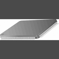
PC87393VJG National Semiconductor, PC87393VJG Datasheet - Page 55

PC87393VJG
Manufacturer Part Number
PC87393VJG
Description
IC, SUPER I/O DEVICE, TQFP-100
Manufacturer
National Semiconductor
Specifications of PC87393VJG
Data Rate
2Mbps
Supply Voltage Range
3V to 3.6V
Logic Case Style
TQFP
No. Of Pins
100
Operating Temperature Range
0°C to +70°C
Termination Type
SMD
Transceiver Type
Interface
Rohs Compliant
No
Available stocks
Company
Part Number
Manufacturer
Quantity
Price
Part Number:
PC87393VJG
Manufacturer:
NS/国半
Quantity:
20 000
- Current page: 55 of 148
- Download datasheet (2Mb)
2.0 Device Architecture and Configuration
2.14 SERIAL PORT 1 CONFIGURATION
2.14.1 Logical Device 3 (SP1) Configuration
Table 22 lists the configuration registers which affect the Serial Port 2. Only the last register (F0h) is described here. See
Sections 2.2.3 and 2.2.4 for descriptions of the others.
2.14.2 Serial Port 1 Configuration Register
This register is reset by hardware to 02h.
Location:
Type:
Bit
Name
Reset
6-3
Bit
7
2
1
0
Index
Bank Select Enable. Enables bank switching for Serial Port 1.
0: Disabled (default).
1: Enabled
Reserved
Busy Indicator. This read only bit can be used by power management software to decide when to power-down
the Serial Port 1 logical device.
0: No transfer in progress (default).
1: Transfer in progress.
Power Mode Control. When the logical device is active in:
0: Low power mode
1: Normal power mode
TRI-STATE Control. When enabled and the device is inactive, the logical device output pins are in TRI-STATE.
0: Disabled (default)
1: Enabled
30h Activate. See also bit 0 of the SIOCF1 register and bit 3 of the SIOCF6 register. R/W
60h Base Address MSB register. Bits 7-3 (for A15-11) are read only, 00000b.
61h Base Address LSB register. Bit 2-0 (for A2-0) are read only, 000b.
70h Interrupt Number and Wake-Up on IRQ Enable register
71h Interrupt Type. Bit 1 is R/W; other bits are read only.
74h Report no DMA Assignment
75h Report no DMA Assignment
F0h Serial Port 1 Configuration register
Serial Port 1 clock disabled. The output signals are set to their default states. The RI input signal can be
programmed to generate an interrupt. Registers are maintained (unlike Active bit in Index 30 that also
prevents access to Serial Port 1 registers).
Serial Port 1 clock enabled. Serial Port 1 is functional when the logical device is active (default).
Index F0h
R/W
Select
Enable
Bank
7
0
6
0
Table 22. Serial Port 1 Configuration Registers
Configuration Register or Action
5
0
Reserved
Description
55
4
0
(Continued)
3
0
Indicator
Busy
2
0
Type
R/W
R/W
R/W
R/W
R/W
RO
RO
Control
Power
Mode
1
1
Reset
00h
03h
F8h
04h
03h
04h
04h
02h
TRI-STATE
www.national.com
Control
0
0
Related parts for PC87393VJG
Image
Part Number
Description
Manufacturer
Datasheet
Request
R
Part Number:
Description:
National Semiconductor [8-Bit D/A Converter]
Manufacturer:
National Semiconductor
Datasheet:
Part Number:
Description:
National Semiconductor [Media Coprocessor]
Manufacturer:
National Semiconductor
Datasheet:
Part Number:
Description:
Digitally Controlled Tone and Volume Circuit with Stereo Audio Power Amplifier, Microphone Preamp Stage and National 3D Sound
Manufacturer:
National Semiconductor
Datasheet:
Part Number:
Description:
Digitally Controlled Tone and Volume Circuit with Stereo Audio Power Amplifier, Microphone Preamp Stage and National 3D Sound
Manufacturer:
National Semiconductor
Datasheet:
Part Number:
Description:
AC97 Rev 2 Codec with Sample Rate Conversion and National 3D Sound
Manufacturer:
National Semiconductor
Part Number:
Description:
Manufacturer:
National Semiconductor
Datasheet:
Part Number:
Description:
Manufacturer:
National Semiconductor
Datasheet:
Part Number:
Description:
General Purpose, Low Voltage, Low Power, Rail-to-Rail Output Operational Amplifiers
Manufacturer:
National Semiconductor
Datasheet:
Part Number:
Description:
8-bit 20 MSPS flash A/D converter.
Manufacturer:
National Semiconductor
Datasheet:
Part Number:
Description:
Low Noise Quad Operational Amplifier
Manufacturer:
National Semiconductor
Datasheet:
Part Number:
Description:
Quad Differential Line Receivers
Manufacturer:
National Semiconductor
Datasheet:
Part Number:
Description:
Quad High Speed Trapezoidal? Bus Transceiver
Manufacturer:
National Semiconductor
Datasheet:
Part Number:
Description:
Dual Line Receiver
Manufacturer:
National Semiconductor
Datasheet:
Part Number:
Description:
TTL to 10k ECL Level Translator with Latch
Manufacturer:
National Semiconductor
Datasheet:


