MA240017 Microchip Technology, MA240017 Datasheet - Page 46
MA240017
Manufacturer Part Number
MA240017
Description
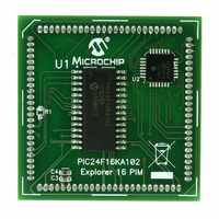
MODULE PLUG-IN PIC24F16KA102 PIM
Manufacturer
Microchip Technology
Series
PIC®r
Specifications of MA240017
Accessory Type
Plug-In Module (PIM) - PIC24F16KA102
Product
Microcontroller Modules
Data Bus Width
16 bit
Core Processor
PIC24F16KA102
Operating Supply Voltage
3 V to 3.6 V
Development Tools By Supplier
Integrated Development Environment, Assembler, ANSI C Compiler
Processor Series
PIC24F
Silicon Manufacturer
Microchip
Core Architecture
PIC
Core Sub-architecture
PIC24
Silicon Core Number
PIC24F
Silicon Family Name
PIC24FxxKAxx
Lead Free Status / RoHS Status
Lead free / RoHS Compliant
For Use With/related Products
Explorer 16 (DM240001 or DM240002)
For Use With
DM240001 - BOARD DEMO PIC24/DSPIC33/PIC32
Lead Free Status / Rohs Status
Lead free / RoHS Compliant
Available stocks
Company
Part Number
Manufacturer
Quantity
Price
Company:

Part Number:
MA240017
Manufacturer:
MICROCHIP
Quantity:
12 000


PIC24F16KA102 FAMILY
5.2
The PIC24F Flash program memory array is organized
into rows of 32 instructions or 96 bytes. RTSP allows
the user to erase blocks of 1 row, 2 rows and 4 rows
(32, 64 and 128 instructions) at a time and to program
one row at a time. It is also possible to program single
words.
The 1-row (96 bytes), 2-row (192 bytes) and 4-row
(384 bytes) erase blocks and single row write block
(96 bytes) are edge-aligned, from the beginning of
program memory.
When data is written to program memory using TBLWT
instructions, the data is not written directly to memory.
Instead, data written using table writes is stored in holding
latches until the programming sequence is executed.
Any number of TBLWT instructions can be executed
and a write will be successfully performed. However,
32 TBLWT instructions are required to write the full row
of memory.
The basic sequence for RTSP programming is to set up
a Table Pointer, then do a series of TBLWT instructions to
load the buffers. Programming is performed by setting
the control bits in the NVMCON register.
Data can be loaded in any order and the holding
registers can be written to multiple times before
performing a write operation. Subsequent writes,
however, will wipe out any previous writes.
All of the table write operations are single-word writes
(two instruction cycles), because only the buffers are
written.
programming each row.
DS39927B-page 44
Note:
RTSP Operation
A
Writing to a location multiple times without
erasing it is not recommended.
programming
cycle
is
required
Preliminary
for
5.3
Enhanced ICSP uses an on-board bootloader, known
as the program executive, to manage the programming
process. Using an SPI data frame format, the program
executive can erase, program and verify program
memory. For more information on Enhanced ICSP, see
the device programming specification.
5.4
There are two SFRs used to read and write the
program Flash memory: NVMCON and NVMKEY.
The NVMCON register (Register 5-1) controls the
blocks that need to be erased, which memory type is to
be programmed and when the programming cycle
starts.
NVMKEY is a write-only register that is used for write
protection. To start a programming or erase sequence,
the user must consecutively write 55h and AAh to the
NVMKEY register. Refer to Section 5.5 “Programming
Operations” for further details.
5.5
A complete programming sequence is necessary for
programming or erasing the internal Flash in RTSP
mode. During a programming or erase operation, the
processor stalls (waits) until the operation is finished.
Setting the WR bit (NVMCON<15>) starts the
operation and the WR bit is automatically cleared when
the operation is finished.
Enhanced In-Circuit Serial
Programming
Control Registers
Programming Operations
© 2009 Microchip Technology Inc.
Related parts for MA240017
Image
Part Number
Description
Manufacturer
Datasheet
Request
R

Part Number:
Description:
Manufacturer:
Microchip Technology Inc.
Datasheet:
Part Number:
Description:
Manufacturer:
Microchip Technology Inc.
Datasheet:
Part Number:
Description:
Manufacturer:
Microchip Technology Inc.
Datasheet:
Part Number:
Description:
Manufacturer:
Microchip Technology Inc.
Datasheet:
Part Number:
Description:
Manufacturer:
Microchip Technology Inc.
Datasheet:
Part Number:
Description:
Manufacturer:
Microchip Technology Inc.
Datasheet:
Part Number:
Description:
Manufacturer:
Microchip Technology Inc.
Datasheet:
Part Number:
Description:
Manufacturer:
Microchip Technology Inc.
Datasheet: