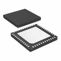
AT91SAM7S32B-MU Atmel, AT91SAM7S32B-MU Datasheet - Page 134

AT91SAM7S32B-MU
Manufacturer Part Number
AT91SAM7S32B-MU
Description
IC MCU ARM7 32KB FLASH 48-VQFN
Manufacturer
Atmel
Series
AT91SAMr
Datasheet
1.AT91SAM7S16-MU.pdf
(779 pages)
Specifications of AT91SAM7S32B-MU
Core Processor
ARM7
Core Size
16/32-Bit
Speed
55MHz
Connectivity
I²C, SPI, SSC, UART/USART
Peripherals
Brown-out Detect/Reset, DMA, POR, PWM, WDT
Number Of I /o
21
Program Memory Size
32KB (32K x 8)
Program Memory Type
FLASH
Ram Size
8K x 8
Voltage - Supply (vcc/vdd)
1.65 V ~ 1.95 V
Data Converters
A/D 8x10b
Oscillator Type
Internal
Operating Temperature
-40°C ~ 85°C
Package / Case
48-VQFN Exposed Pad, 48-HVQFN, 48-SQFN, 48-DHVQFN
For Use With
AT91SAM-ICE - EMULATOR FOR AT91 ARM7/ARM9AT91SAM7S-EK - KIT EVAL FOR ARM AT91SAM7S
Lead Free Status / RoHS Status
Lead free / RoHS Compliant
Eeprom Size
-
Available stocks
Company
Part Number
Manufacturer
Quantity
Price
- Current page: 134 of 779
- Download datasheet (11Mb)
20.2.5.7
20.2.5.8
134
AT91SAM7S Series Preliminary
AT91SAM7S512 Select EFC Command
Memory Write Command
The AT91SAM7S512 security bit is controlled by the EFC0. To use the Set Security Bit com-
mand, the EFC0 must be selected using the Select EFC command
Table 20-15. Set Security Bit Command
Once the security bit is set, it is not possible to access FFPI. The only way to erase the security
bit is to erase the Flash.
In order to erase the Flash, the user must perform the following:
Then it is possible o return to FFPI mode and check that Flash is erased.
The commands WPx, EA, xLB, xFB are executed using the current EFC controller. The default
EFC controller is EFC0. The Select EFC command (SEFC) allows selection of the current EFC
controller.
Table 20-16. Select EFC Command
This command is used to perform a write access to any memory location.
The Memory Write command (WRAM) is optimized for consecutive writes. Write handshaking
can be chained; an internal address buffer is automatically increased.
Table 20-17. Write Command
Step
1
2
Step
1
2
Step
1
2
3
4
5
...
n
n+1
• Power-off the chip
• Power-on the chip with TST = 0
• Assert Erase during a period of more than 220 ms
• Power-off the chip
Handshake Sequence
Write handshaking
Write handshaking
Handshake Sequence
Write handshaking
Write handshaking
Handshake Sequence
Write handshaking
Write handshaking
Write handshaking
Write handshaking
Write handshaking
...
Write handshaking
Write handshaking
MODE[3:0]
CMDE
ADDR0
ADDR1
DATA
DATA
...
ADDR0
ADDR1
MODE[3:0]
CMDE
DATA
MODE[3:0]
CMDE
DATA
DATA[15:0]
WRAM
Memory Address LSB
Memory Address
*Memory Address++
*Memory Address++
...
Memory Address LSB
Memory Address
DATA[15:0]
SEFC
0 = Select EFC0
1 = Select EFC1
DATA[15:0]
SSE
0
6175K–ATARM–30-Aug-10
Related parts for AT91SAM7S32B-MU
Image
Part Number
Description
Manufacturer
Datasheet
Request
R

Part Number:
Description:
KIT EVAL FOR ARM AT91SAM7S
Manufacturer:
Atmel
Datasheet:

Part Number:
Description:
MCU, MPU & DSP Development Tools KICKSTART KIT ATMEL AT91SAM7S
Manufacturer:
IAR Systems

Part Number:
Description:
DEV KIT FOR AVR/AVR32
Manufacturer:
Atmel
Datasheet:

Part Number:
Description:
INTERVAL AND WIPE/WASH WIPER CONTROL IC WITH DELAY
Manufacturer:
ATMEL Corporation
Datasheet:

Part Number:
Description:
Low-Voltage Voice-Switched IC for Hands-Free Operation
Manufacturer:
ATMEL Corporation
Datasheet:

Part Number:
Description:
MONOLITHIC INTEGRATED FEATUREPHONE CIRCUIT
Manufacturer:
ATMEL Corporation
Datasheet:

Part Number:
Description:
AM-FM Receiver IC U4255BM-M
Manufacturer:
ATMEL Corporation
Datasheet:

Part Number:
Description:
Monolithic Integrated Feature Phone Circuit
Manufacturer:
ATMEL Corporation
Datasheet:

Part Number:
Description:
Multistandard Video-IF and Quasi Parallel Sound Processing
Manufacturer:
ATMEL Corporation
Datasheet:

Part Number:
Description:
High-performance EE PLD
Manufacturer:
ATMEL Corporation
Datasheet:

Part Number:
Description:
8-bit Flash Microcontroller
Manufacturer:
ATMEL Corporation
Datasheet:

Part Number:
Description:
2-Wire Serial EEPROM
Manufacturer:
ATMEL Corporation
Datasheet:


