AT91SAM7S32B-MU Atmel, AT91SAM7S32B-MU Datasheet - Page 195
AT91SAM7S32B-MU
Manufacturer Part Number
AT91SAM7S32B-MU
Description
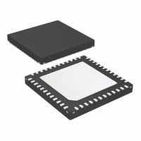
IC MCU ARM7 32KB FLASH 48-VQFN
Manufacturer
Atmel
Series
AT91SAMr
Datasheet
1.AT91SAM7S16-MU.pdf
(779 pages)
Specifications of AT91SAM7S32B-MU
Core Processor
ARM7
Core Size
16/32-Bit
Speed
55MHz
Connectivity
I²C, SPI, SSC, UART/USART
Peripherals
Brown-out Detect/Reset, DMA, POR, PWM, WDT
Number Of I /o
21
Program Memory Size
32KB (32K x 8)
Program Memory Type
FLASH
Ram Size
8K x 8
Voltage - Supply (vcc/vdd)
1.65 V ~ 1.95 V
Data Converters
A/D 8x10b
Oscillator Type
Internal
Operating Temperature
-40°C ~ 85°C
Package / Case
48-VQFN Exposed Pad, 48-HVQFN, 48-SQFN, 48-DHVQFN
For Use With
AT91SAM-ICE - EMULATOR FOR AT91 ARM7/ARM9AT91SAM7S-EK - KIT EVAL FOR ARM AT91SAM7S
Lead Free Status / RoHS Status
Lead free / RoHS Compliant
Eeprom Size
-
Available stocks
Company
Part Number
Manufacturer
Quantity
Price


6175K–ATARM–30-Aug-10
Note:
• If a new value for CSS field corresponds to Main Clock or Slow Clock,
5. Selection of Programmable clocks
If at some stage one of the following parameters, CSS or PRES, is modified, the MCKRDY
bit will go low to indicate that the Master Clock and the Processor Clock are not ready yet.
The user must wait for MCKRDY bit to be set again before using the Master and Processor
Clocks.
Code Example:
The Master Clock is main clock divided by 16.
The Processor Clock is the Master Clock.
Programmable clocks are controlled via registers; PMC_SCER, PMC_SCDR and
PMC_SCSR.
Programmable clocks can be enabled and/or disabled via the PMC_SCER and PMC_SCDR
registers. Depending on the system used, 3 Programmable clocks can be enabled or dis-
abled. The PMC_SCSR provides a clear indication as to which Programmable clock is
enabled. By default all Programmable clocks are disabled.
PMC_PCKx registers are used to configure Programmable clocks.
The CSS field is used to select the Programmable clock divider source. Four clock options
are available: main clock, slow clock, PLLCK. By default, the clock source selected is slow
clock.
The PRES field is used to control the Programmable clock prescaler. It is possible to choose
between different values (1, 2, 4, 8, 16, 32, 64). Programmable clock output is prescaler
input divided by PRES parameter. By default, the PRES parameter is set to 1 which means
that master clock is equal to slow clock.
Once the PMC_PCKx register has been programmed, The corresponding Programmable
clock must be enabled and the user is constrained to wait for the PCKRDYx bit to be set in
the PMC_SR register. This can be done either by polling the status register or by waiting the
– Program the CSS field in the PMC_MCKR register.
– Wait for the MCKRDY bit to be set in the PMC_SR register.
– Program the CSS field in the PMC_MCKR register.
– Wait for the MCKRDY bit to be set in the PMC_SR register.
– Program the PRES field in the PMC_MCKR register.
– Wait for the MCKRDY bit to be set in the PMC_SR register.
write_register(PMC_MCKR,0x00000001)
wait (MCKRDY=1)
write_register(PMC_MCKR,0x00000011)
wait (MCKRDY=1)
IF PLLx clock was selected as the Master Clock and the user decides to modify it by writing in
CKGR_PLLR the MCKRDY flag will go low while PLL is unlocked. Once PLL is locked again,
LOCK goes high and MCKRDY is set.
While PLL is unlocked, the Master Clock selection is automatically changed to Main Clock. For fur-
ther information, see
Section
25.8.2.
AT91SAM7S Series Preliminary
“Clock Switching Waveforms” on page
197.
195
Related parts for AT91SAM7S32B-MU
Image
Part Number
Description
Manufacturer
Datasheet
Request
R

Part Number:
Description:
KIT EVAL FOR ARM AT91SAM7S
Manufacturer:
Atmel
Datasheet:

Part Number:
Description:
MCU, MPU & DSP Development Tools KICKSTART KIT ATMEL AT91SAM7S
Manufacturer:
IAR Systems

Part Number:
Description:
DEV KIT FOR AVR/AVR32
Manufacturer:
Atmel
Datasheet:

Part Number:
Description:
INTERVAL AND WIPE/WASH WIPER CONTROL IC WITH DELAY
Manufacturer:
ATMEL Corporation
Datasheet:
Part Number:
Description:
Low-Voltage Voice-Switched IC for Hands-Free Operation
Manufacturer:
ATMEL Corporation
Datasheet:
Part Number:
Description:
MONOLITHIC INTEGRATED FEATUREPHONE CIRCUIT
Manufacturer:
ATMEL Corporation
Datasheet:
Part Number:
Description:
AM-FM Receiver IC U4255BM-M
Manufacturer:
ATMEL Corporation
Datasheet:
Part Number:
Description:
Monolithic Integrated Feature Phone Circuit
Manufacturer:
ATMEL Corporation
Datasheet:
Part Number:
Description:
Multistandard Video-IF and Quasi Parallel Sound Processing
Manufacturer:
ATMEL Corporation
Datasheet:
Part Number:
Description:
High-performance EE PLD
Manufacturer:
ATMEL Corporation
Datasheet:
Part Number:
Description:
8-bit Flash Microcontroller
Manufacturer:
ATMEL Corporation
Datasheet:
Part Number:
Description:
2-Wire Serial EEPROM
Manufacturer:
ATMEL Corporation
Datasheet: