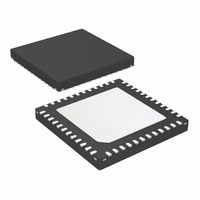
AT91SAM7S32B-MU Atmel, AT91SAM7S32B-MU Datasheet - Page 617

AT91SAM7S32B-MU
Manufacturer Part Number
AT91SAM7S32B-MU
Description
IC MCU ARM7 32KB FLASH 48-VQFN
Manufacturer
Atmel
Series
AT91SAMr
Datasheet
1.AT91SAM7S16-MU.pdf
(779 pages)
Specifications of AT91SAM7S32B-MU
Core Processor
ARM7
Core Size
16/32-Bit
Speed
55MHz
Connectivity
I²C, SPI, SSC, UART/USART
Peripherals
Brown-out Detect/Reset, DMA, POR, PWM, WDT
Number Of I /o
21
Program Memory Size
32KB (32K x 8)
Program Memory Type
FLASH
Ram Size
8K x 8
Voltage - Supply (vcc/vdd)
1.65 V ~ 1.95 V
Data Converters
A/D 8x10b
Oscillator Type
Internal
Operating Temperature
-40°C ~ 85°C
Package / Case
48-VQFN Exposed Pad, 48-HVQFN, 48-SQFN, 48-DHVQFN
For Use With
AT91SAM-ICE - EMULATOR FOR AT91 ARM7/ARM9AT91SAM7S-EK - KIT EVAL FOR ARM AT91SAM7S
Lead Free Status / RoHS Status
Lead free / RoHS Compliant
Eeprom Size
-
Available stocks
Company
Part Number
Manufacturer
Quantity
Price
- Current page: 617 of 779
- Download datasheet (11Mb)
40.6.7
40.6.7.1
40.6.7.2
40.6.7.3
40.6.7.4
6175K–ATARM–30-Aug-10
Pulse Width Modulation Controller (PWM)
PWM: Counter Start Value
PWM: Constraints on Duty Cycle Value
PWM: Update when PWM_CCNTx = 0 or 1
PWM: Update when PWM_CPRDx = 0
Note:
When changing CSS in the PMC_MCKR to switch from
Ensure that the processor is executing out of SRAM and ensure no transition occurs on PA1,
either as an input or output, starting from writing to the PMC_MCKR register until MCKRDY = 1.
If the Channel Counter Register value is 0 or 1, the Channel Period Register or Channel Duty
Cycle Register is directly modified when writing the Channel Update Register.
Check the Channel Counter Register before writing the update register.
When Channel Period Register equals 0, the period update is not operational.
Do not write 0 in the period register.
In left aligned mode, the first start value of the counter is 0. For the other periods, the counter
starts at 1.
None.
Setting Channel Duty Cycle Register (PWM_CDTYx) at 0 in center aligned mode or at 0 or 1 in
left aligned mode may change the polarity of the signal.
Do not set PWM_CDTYx at 0 in center aligned mode.
Do not set PWM_CDTYx at 0 or 1 in left aligned mode.
1. Switching from:
2. Program code is being executed out of flash, or a transition is occurring on PA1, either
And
Problem Fix/Workaround
Problem Fix/Workaround
Problem Fix/Workaround
Problem Fix/Workaround
Problem Fix/Workaround
– PLL Clock to Slow Clock or
– PLL Clock to Main Clock or
– Main Clock to PLL Clock or
– Main Clock to Slow Clock
as an input or output.
– PLL Clock to Slow Clock or
– PLL Clock to Main Clock or
– Main Clock to PLL Clock or
– Main Clock to Slow Clock
This issue does not occur when transitioning from slow clock to main clock or from slow clock to
PLL clock.
AT91SAM7S Series Preliminary
617
Related parts for AT91SAM7S32B-MU
Image
Part Number
Description
Manufacturer
Datasheet
Request
R

Part Number:
Description:
KIT EVAL FOR ARM AT91SAM7S
Manufacturer:
Atmel
Datasheet:

Part Number:
Description:
MCU, MPU & DSP Development Tools KICKSTART KIT ATMEL AT91SAM7S
Manufacturer:
IAR Systems

Part Number:
Description:
DEV KIT FOR AVR/AVR32
Manufacturer:
Atmel
Datasheet:

Part Number:
Description:
INTERVAL AND WIPE/WASH WIPER CONTROL IC WITH DELAY
Manufacturer:
ATMEL Corporation
Datasheet:

Part Number:
Description:
Low-Voltage Voice-Switched IC for Hands-Free Operation
Manufacturer:
ATMEL Corporation
Datasheet:

Part Number:
Description:
MONOLITHIC INTEGRATED FEATUREPHONE CIRCUIT
Manufacturer:
ATMEL Corporation
Datasheet:

Part Number:
Description:
AM-FM Receiver IC U4255BM-M
Manufacturer:
ATMEL Corporation
Datasheet:

Part Number:
Description:
Monolithic Integrated Feature Phone Circuit
Manufacturer:
ATMEL Corporation
Datasheet:

Part Number:
Description:
Multistandard Video-IF and Quasi Parallel Sound Processing
Manufacturer:
ATMEL Corporation
Datasheet:

Part Number:
Description:
High-performance EE PLD
Manufacturer:
ATMEL Corporation
Datasheet:

Part Number:
Description:
8-bit Flash Microcontroller
Manufacturer:
ATMEL Corporation
Datasheet:

Part Number:
Description:
2-Wire Serial EEPROM
Manufacturer:
ATMEL Corporation
Datasheet:


