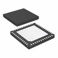
AT91SAM7S32B-MU Atmel, AT91SAM7S32B-MU Datasheet - Page 52

AT91SAM7S32B-MU
Manufacturer Part Number
AT91SAM7S32B-MU
Description
IC MCU ARM7 32KB FLASH 48-VQFN
Manufacturer
Atmel
Series
AT91SAMr
Datasheet
1.AT91SAM7S16-MU.pdf
(779 pages)
Specifications of AT91SAM7S32B-MU
Core Processor
ARM7
Core Size
16/32-Bit
Speed
55MHz
Connectivity
I²C, SPI, SSC, UART/USART
Peripherals
Brown-out Detect/Reset, DMA, POR, PWM, WDT
Number Of I /o
21
Program Memory Size
32KB (32K x 8)
Program Memory Type
FLASH
Ram Size
8K x 8
Voltage - Supply (vcc/vdd)
1.65 V ~ 1.95 V
Data Converters
A/D 8x10b
Oscillator Type
Internal
Operating Temperature
-40°C ~ 85°C
Package / Case
48-VQFN Exposed Pad, 48-HVQFN, 48-SQFN, 48-DHVQFN
For Use With
AT91SAM-ICE - EMULATOR FOR AT91 ARM7/ARM9AT91SAM7S-EK - KIT EVAL FOR ARM AT91SAM7S
Lead Free Status / RoHS Status
Lead free / RoHS Compliant
Eeprom Size
-
Available stocks
Company
Part Number
Manufacturer
Quantity
Price
- Current page: 52 of 779
- Download datasheet (11Mb)
12.5.4
12.5.4.1
52
AT91SAM7S Series Preliminary
IEEE 1149.1 JTAG Boundary Scan
JTAG Boundary-scan Register
Table 12-2.
For further details on the Debug Unit, see the Debug Unit section.
IEEE 1149.1 JTAG Boundary Scan allows pin-level access independent of the device packaging
technology.
IEEE 1149.1 JTAG Boundary Scan is enabled when JTAGSEL is high. The SAMPLE, EXTEST
and BYPASS functions are implemented. In ICE debug mode, the ARM processor responds
with a non-JTAG chip ID that identifies the processor to the ICE system. This is not IEEE 1149.1
JTAG-compliant.
It is not possible to switch directly between JTAG and ICE operations. A chip reset must be per-
formed after JTAGSEL is changed.
A Boundary-scan Descriptor Language (BSDL) file is provided to set up testing.
The Boundary-scan Register (BSR) contains 96 bits that correspond to active pins and associ-
ated control signals.
Each AT91SAM7Sxx input/output pin corresponds to a 3-bit register in the BSR. The OUTPUT
bit contains data that can be forced on the pad. The INPUT bit facilitates the observability of data
applied to the pad. The CONTROL bit selects the direction of the pad.
Table 12-3.
AT91SAM7S64 Rev C
AT91SAM7S128 Rev A
AT91SAM7S128 Rev B
AT91SAM7S128 Rev C
AT91SAM7S256 Rev A
AT91SAM7S256 Rev B
AT91SAM7S256 Rev C
AT91SAM7S512 Rev A and B
Bit Number
96
95
94
93
92
91
AT91SAM7S Series Debug Unit Chip ID (Continued)
AT91SAM7Sxx JTAG Boundary Scan Register
PA17/PGMD5/AD0
PA18/PGMD6/AD1
Pin Name
Pin Type
IN/OUT
IN/OUT
0x270B0A40
0x270C0740
0x270A0741
0x270A0742
0x270D0940
0x270B0941
0x270B0942
0x27090544
6175K–ATARM–30-Aug-10
Associated BSR
CONTROL
CONTROL
OUTPUT
OUTPUT
INPUT
INPUT
Cells
Related parts for AT91SAM7S32B-MU
Image
Part Number
Description
Manufacturer
Datasheet
Request
R

Part Number:
Description:
KIT EVAL FOR ARM AT91SAM7S
Manufacturer:
Atmel
Datasheet:

Part Number:
Description:
MCU, MPU & DSP Development Tools KICKSTART KIT ATMEL AT91SAM7S
Manufacturer:
IAR Systems

Part Number:
Description:
DEV KIT FOR AVR/AVR32
Manufacturer:
Atmel
Datasheet:

Part Number:
Description:
INTERVAL AND WIPE/WASH WIPER CONTROL IC WITH DELAY
Manufacturer:
ATMEL Corporation
Datasheet:

Part Number:
Description:
Low-Voltage Voice-Switched IC for Hands-Free Operation
Manufacturer:
ATMEL Corporation
Datasheet:

Part Number:
Description:
MONOLITHIC INTEGRATED FEATUREPHONE CIRCUIT
Manufacturer:
ATMEL Corporation
Datasheet:

Part Number:
Description:
AM-FM Receiver IC U4255BM-M
Manufacturer:
ATMEL Corporation
Datasheet:

Part Number:
Description:
Monolithic Integrated Feature Phone Circuit
Manufacturer:
ATMEL Corporation
Datasheet:

Part Number:
Description:
Multistandard Video-IF and Quasi Parallel Sound Processing
Manufacturer:
ATMEL Corporation
Datasheet:

Part Number:
Description:
High-performance EE PLD
Manufacturer:
ATMEL Corporation
Datasheet:

Part Number:
Description:
8-bit Flash Microcontroller
Manufacturer:
ATMEL Corporation
Datasheet:

Part Number:
Description:
2-Wire Serial EEPROM
Manufacturer:
ATMEL Corporation
Datasheet:


