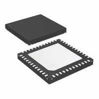
AT91SAM7S32B-MU Atmel, AT91SAM7S32B-MU Datasheet - Page 510

AT91SAM7S32B-MU
Manufacturer Part Number
AT91SAM7S32B-MU
Description
IC MCU ARM7 32KB FLASH 48-VQFN
Manufacturer
Atmel
Series
AT91SAMr
Datasheet
1.AT91SAM7S16-MU.pdf
(779 pages)
Specifications of AT91SAM7S32B-MU
Core Processor
ARM7
Core Size
16/32-Bit
Speed
55MHz
Connectivity
I²C, SPI, SSC, UART/USART
Peripherals
Brown-out Detect/Reset, DMA, POR, PWM, WDT
Number Of I /o
21
Program Memory Size
32KB (32K x 8)
Program Memory Type
FLASH
Ram Size
8K x 8
Voltage - Supply (vcc/vdd)
1.65 V ~ 1.95 V
Data Converters
A/D 8x10b
Oscillator Type
Internal
Operating Temperature
-40°C ~ 85°C
Package / Case
48-VQFN Exposed Pad, 48-HVQFN, 48-SQFN, 48-DHVQFN
For Use With
AT91SAM-ICE - EMULATOR FOR AT91 ARM7/ARM9AT91SAM7S-EK - KIT EVAL FOR ARM AT91SAM7S
Lead Free Status / RoHS Status
Lead free / RoHS Compliant
Eeprom Size
-
Available stocks
Company
Part Number
Manufacturer
Quantity
Price
- Current page: 510 of 779
- Download datasheet (11Mb)
Figure 35-11. Data OUT Transfer for Ping-pong Endpoint
Note:
35.5.2.8
510
USB Bus
Packets
RX_DATA_BK0 Flag
(UDP_CSRx)
RX_DATA_BK1 Flag
(UDP_CSRx)
FIFO (DPR)
Bank 0
FIFO (DPR)
Bank 1
An interrupt is pending while the RX_DATA_BK0 or RX_DATA_BK1 flag is set.
AT91SAM7S Series Preliminary
Stall Handshake
Host Sends First Data Payload
Data OUT
PID
Set by USB Device,
Data Payload Written
in FIFO Endpoint Bank 0
Write by USB Device
Data OUT1
Warning: When RX_DATA_BK0 and RX_DATA_BK1 are both set, there is no way to determine
which one to clear first. Thus the software must keep an internal counter to be sure to clear alter-
natively RX_DATA_BK0 then RX_DATA_BK1. This situation may occur when the software
application is busy elsewhere and the two banks are filled by the USB host. Once the application
comes back to the USB driver, the two flags are set.
A stall handshake can be used in one of two distinct occasions. (For more information on the
stall handshake, refer to Chapter 8 of the Universal Serial Bus Specification, Rev 2.0.)
The following procedure generates a stall packet:
11. The microcontroller notifies the USB device it has finished the transfer by clearing
12. A fourth Data OUT packet can be accepted by the USB device and copied in the FIFO
• A functional stall is used when the halt feature associated with the endpoint is set. (Refer to
• To abort the current request, a protocol stall is used, but uniquely with control transfer.
1. The microcontroller sets the FORCESTALL flag in the UDP_ CSRx endpoint’s register.
2. The host receives the stall packet.
Chapter 9 of the Universal Serial Bus Specification, Rev 2.0, for more information on the halt
feature.)
RX_DATA_BK1 in the endpoint’s UDP_ CSRx register.
Bank 0.
Data OUT 1
ACK
PID
Read By Microcontroller
Set by USB Device,
Data Payload Written
in FIFO Endpoint Bank 1
Interrupt Pending
Microcontroller Reads Data 1 in Bank 0,
Host Sends Second Data Payload
Data OUT 1
Data OUT
PID
Write by USB Device
Data OUT 2
Data OUT 2
Cleared by Firmware
ACK
PID
Read By Microcontroller
Data OUT
Microcontroller Reads Data2 in Bank 1,
Host Sends Third Data Payload
PID
Interrupt Pending
Data OUT 2
Write In Progress
Cleared by Firmware
6175K–ATARM–30-Aug-10
Data OUT 3
Data OUT 3
A
P
Related parts for AT91SAM7S32B-MU
Image
Part Number
Description
Manufacturer
Datasheet
Request
R

Part Number:
Description:
KIT EVAL FOR ARM AT91SAM7S
Manufacturer:
Atmel
Datasheet:

Part Number:
Description:
MCU, MPU & DSP Development Tools KICKSTART KIT ATMEL AT91SAM7S
Manufacturer:
IAR Systems

Part Number:
Description:
DEV KIT FOR AVR/AVR32
Manufacturer:
Atmel
Datasheet:

Part Number:
Description:
INTERVAL AND WIPE/WASH WIPER CONTROL IC WITH DELAY
Manufacturer:
ATMEL Corporation
Datasheet:

Part Number:
Description:
Low-Voltage Voice-Switched IC for Hands-Free Operation
Manufacturer:
ATMEL Corporation
Datasheet:

Part Number:
Description:
MONOLITHIC INTEGRATED FEATUREPHONE CIRCUIT
Manufacturer:
ATMEL Corporation
Datasheet:

Part Number:
Description:
AM-FM Receiver IC U4255BM-M
Manufacturer:
ATMEL Corporation
Datasheet:

Part Number:
Description:
Monolithic Integrated Feature Phone Circuit
Manufacturer:
ATMEL Corporation
Datasheet:

Part Number:
Description:
Multistandard Video-IF and Quasi Parallel Sound Processing
Manufacturer:
ATMEL Corporation
Datasheet:

Part Number:
Description:
High-performance EE PLD
Manufacturer:
ATMEL Corporation
Datasheet:

Part Number:
Description:
8-bit Flash Microcontroller
Manufacturer:
ATMEL Corporation
Datasheet:

Part Number:
Description:
2-Wire Serial EEPROM
Manufacturer:
ATMEL Corporation
Datasheet:


