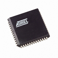
AT89C51CC03C-S3RIM Atmel, AT89C51CC03C-S3RIM Datasheet - Page 169

AT89C51CC03C-S3RIM
Manufacturer Part Number
AT89C51CC03C-S3RIM
Description
IC 8051 MCU FLASH 64K 52PLCC
Manufacturer
Atmel
Series
AT89C CANr
Datasheets
1.AT89C51CC03C-S3RIM.pdf
(198 pages)
2.AT89C51CC03C-S3RIM.pdf
(32 pages)
3.AT89C51CC03C-S3RIM.pdf
(27 pages)
4.AT89C51CC03C-S3RIM.pdf
(184 pages)
Specifications of AT89C51CC03C-S3RIM
Core Processor
8051
Core Size
8-Bit
Speed
40MHz
Connectivity
CAN, SPI, UART/USART
Peripherals
POR, PWM, WDT
Number Of I /o
36
Program Memory Size
64KB (64K x 8)
Program Memory Type
FLASH
Eeprom Size
2K x 8
Ram Size
2.25K x 8
Voltage - Supply (vcc/vdd)
3 V ~ 5.5 V
Data Converters
A/D 8x10b
Oscillator Type
External
Operating Temperature
-40°C ~ 85°C
Package / Case
52-PLCC
Lead Free Status / RoHS Status
Contains lead / RoHS non-compliant
Other names
AT89C51CC03CS3RTR
Available stocks
Company
Part Number
Manufacturer
Quantity
Price
- AT89C51CC03C-S3RIM PDF datasheet
- AT89C51CC03C-S3RIM PDF datasheet #2
- AT89C51CC03C-S3RIM PDF datasheet #3
- AT89C51CC03C-S3RIM PDF datasheet #4
- Current page: 169 of 198
- Download datasheet (3Mb)
Table 116. DC Parameters in Standard Voltage (Continued)
Notes:
4182O–CAN–09/08
Symbol
I
CCWRITE
V
R
V
C
I
I
I
OH1
I
I
RST
PD
CC
TL
OH
IL
LI
IO
1. Operating I
2. Idle I
3. Power-down I
4. Capacitance loading on Ports 0 and 2 may cause spurious noise pulses to be superimposed on the V
5. Typicals are based on a limited number of samples and are not guaranteed. The values listed are at room temperature.
6. Under steady state (non-transient) conditions, I
V
V
78.).
0.5V; XTAL2 N.C; Port 0 = V
ure 80.). In addition, the WDT must be inactive and the POF flag must be set.
and 3. The noise is due to external bus capacitance discharging into the Port 0 and Port 2 pins when these pins make 1 to 0
transitions during bus operation. In the worst cases (capacitive loading 100pF), the noise pulse on the ALE line may exceed
0.45V with maxi V
Maximum I
Maximum I
Port 0: 26 mA
Ports 1, 2, 3 and 4: 15 mA
Maximum total I
If I
than the listed test conditions.
Parameter
Output High Voltage, ports 1, 2, 3, and 4
Output High Voltage, port 0, ALE, PSEN
RST Pulldown Resistor
Logical 0 Input Current ports 1, 2, 3 and 4
Input Leakage Current
Logical 1 to 0 Transition Current, ports 1, 2, 3
and 4
Capacitance of I/O Buffer
Power-down Current Industrial
Power-down Current Automotive
Power Supply Current
Power Supply Current on flash or EEdata write
SS
IH
OL
= V
+ 0.5V,
CC
exceeds the test condition, V
CC
is measured with all output pins disconnected; XTAL1 driven with T
- 0.5V; XTAL2 N.C.; EA = RST = Port 0 = V
OL
OL
CC
CC
per port pin: 10 mA
per 8-bit port:
is measured with all output pins disconnected; XTAL1 driven with T
OL
is measured with all output pins disconnected; EA = V
OL
for all output pins: 71 mA
peak 0.6V. A Schmitt Trigger use is not necessary.
CC
; EA = RST = V
OL
may exceed the related specification. Pins are not guaranteed to sink current greater
I
I
CCOP
CCIDLE
SS
OL
(see Figure 79.).
V
V
V
V
V
V
must be externally limited as follows:
CC
CC
CC
CC
CC
CC
Min
= 0.4 Frequency (MHz) + 8
20
= 0.2 Frequency (MHz) + 8
- 0.3
- 0.7
- 1.5
- 0.3
- 0.7
- 1.5
CC
. I
CC
would be slightly higher if a crystal oscillator used (see Figure
Typ
100
100
75
(5)
CC
, PORT 0 = V
CLCH
(MHz) + 15
Frequency
, T
Max
0.8 x
-650
200
150
350
±10
-50
CLCH
10
CHCL
, T
CC
= 5 ns, V
CHCL
; XTAL2 NC.; RST = V
AT89C51CC03
Unit
mA
mA
kΩ
μA
μA
μA
pF
μA
μA
= 5 ns (see Figure 81.), V
V
V
V
V
V
V
IL
= V
I
I
I
V
I
I
I
V
Vin = 0.45V
0.45V < Vin < V
Vin = 2.0V
Fc = 1 MHz
T
3V < V
3V < V
Vcc = 5.5V
V
OH
OH
OH
OH
OH
OH
A
CC
CC
CC
OL
= 25°C
SS
= -10 μA
= -30 μA
= -60 μA
= -200 μA
= -3.2 mA
= -7.0 mA
s of ALE and Ports 1
= 3V to 5.5V
= 5V ± 10%
= 5.5V
Test Conditions
+ 0.5V, V
CC
CC
< 5.5V
< 5.5V
(1)(2)
SS
CC
(3)
(3)
IH
(see Fig-
= V
169
CC
IL
=
-
Related parts for AT89C51CC03C-S3RIM
Image
Part Number
Description
Manufacturer
Datasheet
Request
R

Part Number:
Description:
Manufacturer:
Atmel Corporation
Datasheet:

Part Number:
Description:
At89c51cc03 Enhanced 8-bit Mcu With Can Controller And Flash Memory
Manufacturer:
ATMEL Corporation
Datasheet:

Part Number:
Description:
DEV KIT FOR AVR/AVR32
Manufacturer:
Atmel
Datasheet:

Part Number:
Description:
INTERVAL AND WIPE/WASH WIPER CONTROL IC WITH DELAY
Manufacturer:
ATMEL Corporation
Datasheet:

Part Number:
Description:
Low-Voltage Voice-Switched IC for Hands-Free Operation
Manufacturer:
ATMEL Corporation
Datasheet:

Part Number:
Description:
MONOLITHIC INTEGRATED FEATUREPHONE CIRCUIT
Manufacturer:
ATMEL Corporation
Datasheet:

Part Number:
Description:
AM-FM Receiver IC U4255BM-M
Manufacturer:
ATMEL Corporation
Datasheet:

Part Number:
Description:
Monolithic Integrated Feature Phone Circuit
Manufacturer:
ATMEL Corporation
Datasheet:

Part Number:
Description:
Multistandard Video-IF and Quasi Parallel Sound Processing
Manufacturer:
ATMEL Corporation
Datasheet:

Part Number:
Description:
High-performance EE PLD
Manufacturer:
ATMEL Corporation
Datasheet:

Part Number:
Description:
8-bit Flash Microcontroller
Manufacturer:
ATMEL Corporation
Datasheet:

Part Number:
Description:
2-Wire Serial EEPROM
Manufacturer:
ATMEL Corporation
Datasheet:


