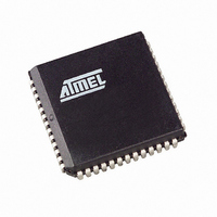
AT89C51CC03C-S3RIM Atmel, AT89C51CC03C-S3RIM Datasheet - Page 171

AT89C51CC03C-S3RIM
Manufacturer Part Number
AT89C51CC03C-S3RIM
Description
IC 8051 MCU FLASH 64K 52PLCC
Manufacturer
Atmel
Series
AT89C CANr
Datasheets
1.AT89C51CC03C-S3RIM.pdf
(198 pages)
2.AT89C51CC03C-S3RIM.pdf
(32 pages)
3.AT89C51CC03C-S3RIM.pdf
(27 pages)
4.AT89C51CC03C-S3RIM.pdf
(184 pages)
Specifications of AT89C51CC03C-S3RIM
Core Processor
8051
Core Size
8-Bit
Speed
40MHz
Connectivity
CAN, SPI, UART/USART
Peripherals
POR, PWM, WDT
Number Of I /o
36
Program Memory Size
64KB (64K x 8)
Program Memory Type
FLASH
Eeprom Size
2K x 8
Ram Size
2.25K x 8
Voltage - Supply (vcc/vdd)
3 V ~ 5.5 V
Data Converters
A/D 8x10b
Oscillator Type
External
Operating Temperature
-40°C ~ 85°C
Package / Case
52-PLCC
Lead Free Status / RoHS Status
Contains lead / RoHS non-compliant
Other names
AT89C51CC03CS3RTR
Available stocks
Company
Part Number
Manufacturer
Quantity
Price
- AT89C51CC03C-S3RIM PDF datasheet
- AT89C51CC03C-S3RIM PDF datasheet #2
- AT89C51CC03C-S3RIM PDF datasheet #3
- AT89C51CC03C-S3RIM PDF datasheet #4
- Current page: 171 of 198
- Download datasheet (3Mb)
DC Parameters for A/D
Converter
AC Parameters
Explanation of the AC
Symbols
4182O–CAN–09/08
Figure 81. Clock Signal Waveform for I
Table 117. DC Parameters for AD Converter in Precision Conversion
Note:
Each timing symbol has 5 characters. The first character is always a “T” (stands for
time). The other characters, depending on their positions, stand for the name of a signal
or the logical status of that signal. The following is a list of all the characters and what
they stand for.
Example: T
T
(Load Capacitance for port 0, ALE and PSEN = 60 pF; Load Capacitance for all other
outputs = 60 pF.)
Table 118, Table 121 and Table 124 give the description of each AC symbols.
Table 119, Table 123 and Table 125 give for each range the AC parameter.
Table 120, Table 123 and Table 126 give the frequency derating formula of the AC
parameter for each speed range description. To calculate each AC symbols: Take the x
value and use this value in the formula.
Example: T
x = 30 ns
T = 50 ns
T
Symbol Parameter
A
CCIV
Vref
T
AVin
Rref
DNL
= -40°C to +85°C; V
Cai
Rai
INL
OE
LLPL
(3)
= 4T - x = 170 ns
= Time for ALE Low to PSEN Low.
1. Typicals are based on a limited number of samples and are not guaranteed.
2. For temperatures higher than 85°C, use standard conversion (8-bit only) and
3. V
Analog input voltage
Resistance between Vref and Vss
Reference voltage
Analog input Capacitance
Analog input Resistor
Integral non linearity
Differential non linearity
Offset error
PRS > 2.
AVLL
LLIV
REF
and 20 MHz, Standard clock.
= Time for Address Valid to ALE Low.
< V
CC
+ 0.2V for temperatures higher than 85.
SS
V
CC
= 0V; V
T
-0.5V
0.45V
CHCL
T
CLCH
CC
= T
= 3V to 5.5V; F = 0 to 40 MHz.
CHCL
Vss- 0.2
CC
Min
2.40
12
-2
= 5ns.
Tests in Active and Idle Modes
T
CLCH
Typ
0.7V
0.2V
0.5
16
60
(1),(2)
1
CC
CC
-0.1
Vref
Max
AT89C51CC03
3.00
400
24
2
3
1
2
+ 0.2
Unit
kΩ
pF During sampling
lsb
lsb
lsb
Ω
V
V
During sampling
Automotive
Test Conditions
171
Related parts for AT89C51CC03C-S3RIM
Image
Part Number
Description
Manufacturer
Datasheet
Request
R

Part Number:
Description:
Manufacturer:
Atmel Corporation
Datasheet:

Part Number:
Description:
At89c51cc03 Enhanced 8-bit Mcu With Can Controller And Flash Memory
Manufacturer:
ATMEL Corporation
Datasheet:

Part Number:
Description:
DEV KIT FOR AVR/AVR32
Manufacturer:
Atmel
Datasheet:

Part Number:
Description:
INTERVAL AND WIPE/WASH WIPER CONTROL IC WITH DELAY
Manufacturer:
ATMEL Corporation
Datasheet:

Part Number:
Description:
Low-Voltage Voice-Switched IC for Hands-Free Operation
Manufacturer:
ATMEL Corporation
Datasheet:

Part Number:
Description:
MONOLITHIC INTEGRATED FEATUREPHONE CIRCUIT
Manufacturer:
ATMEL Corporation
Datasheet:

Part Number:
Description:
AM-FM Receiver IC U4255BM-M
Manufacturer:
ATMEL Corporation
Datasheet:

Part Number:
Description:
Monolithic Integrated Feature Phone Circuit
Manufacturer:
ATMEL Corporation
Datasheet:

Part Number:
Description:
Multistandard Video-IF and Quasi Parallel Sound Processing
Manufacturer:
ATMEL Corporation
Datasheet:

Part Number:
Description:
High-performance EE PLD
Manufacturer:
ATMEL Corporation
Datasheet:

Part Number:
Description:
8-bit Flash Microcontroller
Manufacturer:
ATMEL Corporation
Datasheet:

Part Number:
Description:
2-Wire Serial EEPROM
Manufacturer:
ATMEL Corporation
Datasheet:


