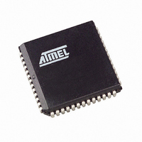
AT89C51CC03C-S3RIM Atmel, AT89C51CC03C-S3RIM Datasheet - Page 23

AT89C51CC03C-S3RIM
Manufacturer Part Number
AT89C51CC03C-S3RIM
Description
IC 8051 MCU FLASH 64K 52PLCC
Manufacturer
Atmel
Series
AT89C CANr
Datasheets
1.AT89C51CC03C-S3RIM.pdf
(198 pages)
2.AT89C51CC03C-S3RIM.pdf
(32 pages)
3.AT89C51CC03C-S3RIM.pdf
(27 pages)
4.AT89C51CC03C-S3RIM.pdf
(184 pages)
Specifications of AT89C51CC03C-S3RIM
Core Processor
8051
Core Size
8-Bit
Speed
40MHz
Connectivity
CAN, SPI, UART/USART
Peripherals
POR, PWM, WDT
Number Of I /o
36
Program Memory Size
64KB (64K x 8)
Program Memory Type
FLASH
Eeprom Size
2K x 8
Ram Size
2.25K x 8
Voltage - Supply (vcc/vdd)
3 V ~ 5.5 V
Data Converters
A/D 8x10b
Oscillator Type
External
Operating Temperature
-40°C ~ 85°C
Package / Case
52-PLCC
Lead Free Status / RoHS Status
Contains lead / RoHS non-compliant
Other names
AT89C51CC03CS3RTR
Available stocks
Company
Part Number
Manufacturer
Quantity
Price
- AT89C51CC03C-S3RIM PDF datasheet
- AT89C51CC03C-S3RIM PDF datasheet #2
- AT89C51CC03C-S3RIM PDF datasheet #3
- AT89C51CC03C-S3RIM PDF datasheet #4
- Current page: 23 of 198
- Download datasheet (3Mb)
Internal Space
Lower 128 Bytes RAM
Upper 128 Bytes RAM
Expanded RAM
4182O–CAN–09/08
The lower 128 Bytes of RAM (see Figure 8) are accessible from address 00h to 7Fh
using direct or indirect addressing modes. The lowest 32 Bytes are grouped into 4
banks of 8 registers (R0 to R7). Two bits RS0 and RS1 in PSW register (see Figure 6)
select which bank is in use according to Table 4. This allows more efficient use of code
space, since register instructions are shorter than instructions that use direct address-
ing, and can be used for context switching in interrupt service routines.
Table 4. Register Bank Selection
The next 16 Bytes above the register banks form a block of bit-addressable memory
space. The C51 instruction set includes a wide selection of single-bit instructions, and
the 128 bits in this area can be directly addressed by these instructions. The bit
addresses in this area are 00h to 7Fh.
Figure 9. Lower 128 Bytes Internal RAM Organization
The upper 128 Bytes of RAM are accessible from address 80h to FFh using only indirect
addressing mode.
The on-chip 2048 Bytes of expanded RAM (ERAM) are accessible from address 0000h
to 07FFh using indirect addressing mode through MOVX instructions. In this address
range, the bit EXTRAM in AUXR register is used to select the ERAM (default) or the
XRAM. As shown in Figure 8 when EXTRAM = 0, the ERAM is selected and when
EXTRAM = 1, the XRAM is selected.
The size of ERAM can be configured by XRS2-0 bit in AUXR register (default size is
2048 Bytes).
Note:
RS1
Lower 128 Bytes RAM, Upper 128 Bytes RAM, and expanded RAM are made of volatile
memory cells. This means that the RAM content is indeterminate after power-up and
must then be initialized properly.
0
0
1
1
RS0
0
1
0
1
30h
20h
18h
10h
08h
00h
Description
Register bank 0 from 00h to 07h
Register bank 0 from 08h to 0Fh
Register bank 0 from 10h to 17h
Register bank 0 from 18h to 1Fh
7Fh
2Fh
1Fh
0Fh
17h
07h
Bit-Addressable Space
(Bit Addresses 0-7Fh)
4 Banks of
8 Registers
R0-R7
AT89C51CC03
23
Related parts for AT89C51CC03C-S3RIM
Image
Part Number
Description
Manufacturer
Datasheet
Request
R

Part Number:
Description:
Manufacturer:
Atmel Corporation
Datasheet:

Part Number:
Description:
At89c51cc03 Enhanced 8-bit Mcu With Can Controller And Flash Memory
Manufacturer:
ATMEL Corporation
Datasheet:

Part Number:
Description:
DEV KIT FOR AVR/AVR32
Manufacturer:
Atmel
Datasheet:

Part Number:
Description:
INTERVAL AND WIPE/WASH WIPER CONTROL IC WITH DELAY
Manufacturer:
ATMEL Corporation
Datasheet:

Part Number:
Description:
Low-Voltage Voice-Switched IC for Hands-Free Operation
Manufacturer:
ATMEL Corporation
Datasheet:

Part Number:
Description:
MONOLITHIC INTEGRATED FEATUREPHONE CIRCUIT
Manufacturer:
ATMEL Corporation
Datasheet:

Part Number:
Description:
AM-FM Receiver IC U4255BM-M
Manufacturer:
ATMEL Corporation
Datasheet:

Part Number:
Description:
Monolithic Integrated Feature Phone Circuit
Manufacturer:
ATMEL Corporation
Datasheet:

Part Number:
Description:
Multistandard Video-IF and Quasi Parallel Sound Processing
Manufacturer:
ATMEL Corporation
Datasheet:

Part Number:
Description:
High-performance EE PLD
Manufacturer:
ATMEL Corporation
Datasheet:

Part Number:
Description:
8-bit Flash Microcontroller
Manufacturer:
ATMEL Corporation
Datasheet:

Part Number:
Description:
2-Wire Serial EEPROM
Manufacturer:
ATMEL Corporation
Datasheet:


