PIC32MX440F512H-80I/MR Microchip Technology, PIC32MX440F512H-80I/MR Datasheet - Page 43
PIC32MX440F512H-80I/MR
Manufacturer Part Number
PIC32MX440F512H-80I/MR
Description
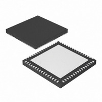
IC PIC MCU FLASH 512KX32 64-QFN
Manufacturer
Microchip Technology
Series
PIC® 32MXr
Datasheets
1.MA320002.pdf
(208 pages)
2.DM320001.pdf
(44 pages)
3.PIC32MX320F032H-40IPT.pdf
(48 pages)
4.PIC32MX320F032H-40IPT.pdf
(66 pages)
5.PIC32MX320F032H-40IPT.pdf
(22 pages)
6.PIC32MX320F064H-40IMR.pdf
(172 pages)
Specifications of PIC32MX440F512H-80I/MR
Core Size
32-Bit
Program Memory Size
512KB (512K x 8)
Core Processor
MIPS32® M4K™
Speed
80MHz
Connectivity
I²C, IrDA, LIN, PMP, SPI, UART/USART, USB OTG
Peripherals
Brown-out Detect/Reset, DMA, POR, PWM, WDT
Number Of I /o
53
Program Memory Type
FLASH
Ram Size
32K x 8
Voltage - Supply (vcc/vdd)
2.3 V ~ 3.6 V
Data Converters
A/D 16x10b
Oscillator Type
Internal
Operating Temperature
-40°C ~ 85°C
Package / Case
64-VFQFN, Exposed Pad
Controller Family/series
PIC32
Ram Memory Size
32KB
Cpu Speed
80MHz
No. Of Timers
5
Interface
EUSART, I2C, SPI, USB
No. Of Pwm Channels
5
Embedded Interface Type
EUSART, I2C, SPI, USB
Rohs Compliant
Yes
Processor Series
PIC32MX4xx
Core
MIPS
Data Bus Width
32 bit
Data Ram Size
32 KB
Interface Type
I2C, JTAG, SPI, TWI, UART, USB
Maximum Clock Frequency
80 MHz
Number Of Programmable I/os
51
Number Of Timers
5
Operating Supply Voltage
2.3 V to 3.6 V
Maximum Operating Temperature
+ 125 C
Mounting Style
SMD/SMT
3rd Party Development Tools
52713-733, 52714-737
Development Tools By Supplier
PG164130, DV164035, DV244005, DV164005, DM320003, DM320002, MA320002
Minimum Operating Temperature
- 40 C
On-chip Adc
10 bit
Lead Free Status / RoHS Status
Lead free / RoHS Compliant
For Use With
876-1000 - PIC32 BREAKOUT BOARD
Eeprom Size
-
Lead Free Status / Rohs Status
Details


TABLE 4-9:
TABLE 4-10:
TABLE 4-11:
Legend:
Note
Legend:
Note
Legend:
Note
BF80_9130 ADC1BUFC
BF80_9140 ADC1BUFD
BF80_9150 ADC1BUFE
BF80_9160 ADC1BUFF
BF88_3000 DMACON
BF88_3010 DMASTAT
BF88_3020 DMAADDR
BF88_3030 DCRCCON
BF88_3040 DCRCDATA
BF88_3050 DCRCXOR
Virtual
Virtual
Virtual
Addr
Addr
Addr
SFR
SFR
SFR
1:
1:
1:
x = unknown value on Reset, — = unimplemented, read as ‘0’. Reset values are shown in hexadecimal.
This register has corresponding CLR, SET, and INV Registers at its virtual address, plus an offset of 0x4, 0x8, and 0xC, respectively. See Section 12.1.1 “CLR, SET and INV Registers” for more information.
x = unknown value on Reset, — = unimplemented, read as ‘0’. Reset values are shown in hexadecimal.
All registers in this table have corresponding CLR, SET, and INV Registers at their virtual addresses, plus offsets of 0x4, 0x8, and 0xC, respectively. See Section 12.1.1 “CLR, SET and INV Registers” for more infor-
mation.
Name
Name
Name
SFR
SFR
SFR
(1)
ADC REGISTERS MAP (CONTINUED)
DMA GLOBAL REGISTERS MAP FOR PIC32MX340FXXXX/360FXXXX/440FXXXX/460XXXX DEVICES ONLY
DMA CRC REGISTERS MAP FOR PIC32MX340FXXXX/360FXXXX/440FXXXX/460XXXX DEVICES ONLY
31:16
31:16
31:16
31:16
31:16
31:16
31:16
31:16
31:16
31:16
15:0
15:0
15:0
15:0
15:0
15:0
15:0
15:0
15:0
15:0
31/15
31/15
31/15
Bits
Bits
Bits
ON
—
—
—
—
—
—
—
30/14
30/14
30/14
Bits
Bits
Bits
FRZ
—
—
—
—
—
—
—
29/13
29/13
29/13
SIDL
Bits
Bits
Bits
—
—
—
—
—
—
—
SUSPEND
28/12
28/12
28/12
Bits
Bits
Bits
—
—
—
—
—
—
—
27/11
27/11
27/11
Bits
Bits
Bits
—
—
—
—
—
—
—
26/10
26/10
26/10
Bits
Bits
Bits
—
—
—
—
—
—
—
PLEN<3:0>
25/9
ADC Result Word C (ADC1BUFC<31:0>)
ADC Result Word D (ADC1BUFD<31:0>)
25/9
25/9
Bits
ADC Result Word E (ADC1BUFE<31:0>)
ADC Result Word F (ADC1BUFF<31:0>)
Bits
Bits
—
—
—
—
—
—
—
DCRCDATA<15:0>
DMAADDR<31:0>
DCRCXOR<15:0>
Bits
24/8
Bits
24/8
Bits
24/8
—
—
—
—
—
—
—
CRCEN
Bits
23/7
Bits
23/7
Bits
23/7
—
—
—
—
—
—
—
CRCAPP
Bits
22/6
Bits
22/6
Bits
22/6
—
—
—
—
—
—
—
Bits
21/5
Bits
21/5
Bits
21/5
—
—
—
—
—
—
—
—
20/4
20/4
20/4
Bits
Bits
Bits
—
—
—
—
—
—
—
—
RDWR
19/3
19/3
19/3
Bits
Bits
Bits
—
—
—
—
—
—
—
(1)
18/2
18/2
18/2
Bits
Bits
Bits
—
—
—
—
—
—
—
—
Bits
17/1
Bits
17/1
Bits
17/1
—
—
—
DMACH<1:0>
—
—
—
CRCCH<1:0>
Bits
16/0
Bits
16/0
Bits
16/0
—
—
—
—
—
—
Related parts for PIC32MX440F512H-80I/MR
Image
Part Number
Description
Manufacturer
Datasheet
Request
R

Part Number:
Description:
Manufacturer:
Microchip Technology Inc.
Datasheet:
Part Number:
Description:
Manufacturer:
Microchip Technology Inc.
Datasheet:
Part Number:
Description:
Manufacturer:
Microchip Technology Inc.
Datasheet:
Part Number:
Description:
Manufacturer:
Microchip Technology Inc.
Datasheet:
Part Number:
Description:
Manufacturer:
Microchip Technology Inc.
Datasheet:
Part Number:
Description:
Manufacturer:
Microchip Technology Inc.
Datasheet:
Part Number:
Description:
Manufacturer:
Microchip Technology Inc.
Datasheet:
Part Number:
Description:
Manufacturer:
Microchip Technology Inc.
Datasheet: