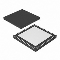
PIC32MX440F512H-80I/MR Microchip Technology, PIC32MX440F512H-80I/MR Datasheet - Page 73

PIC32MX440F512H-80I/MR
Manufacturer Part Number
PIC32MX440F512H-80I/MR
Description
IC PIC MCU FLASH 512KX32 64-QFN
Manufacturer
Microchip Technology
Series
PIC® 32MXr
Datasheets
1.MA320002.pdf
(208 pages)
2.DM320001.pdf
(44 pages)
3.PIC32MX320F032H-40IPT.pdf
(48 pages)
4.PIC32MX320F032H-40IPT.pdf
(66 pages)
5.PIC32MX320F032H-40IPT.pdf
(22 pages)
6.PIC32MX320F064H-40IMR.pdf
(172 pages)
Specifications of PIC32MX440F512H-80I/MR
Core Size
32-Bit
Program Memory Size
512KB (512K x 8)
Core Processor
MIPS32® M4K™
Speed
80MHz
Connectivity
I²C, IrDA, LIN, PMP, SPI, UART/USART, USB OTG
Peripherals
Brown-out Detect/Reset, DMA, POR, PWM, WDT
Number Of I /o
53
Program Memory Type
FLASH
Ram Size
32K x 8
Voltage - Supply (vcc/vdd)
2.3 V ~ 3.6 V
Data Converters
A/D 16x10b
Oscillator Type
Internal
Operating Temperature
-40°C ~ 85°C
Package / Case
64-VFQFN, Exposed Pad
Controller Family/series
PIC32
Ram Memory Size
32KB
Cpu Speed
80MHz
No. Of Timers
5
Interface
EUSART, I2C, SPI, USB
No. Of Pwm Channels
5
Embedded Interface Type
EUSART, I2C, SPI, USB
Rohs Compliant
Yes
Processor Series
PIC32MX4xx
Core
MIPS
Data Bus Width
32 bit
Data Ram Size
32 KB
Interface Type
I2C, JTAG, SPI, TWI, UART, USB
Maximum Clock Frequency
80 MHz
Number Of Programmable I/os
51
Number Of Timers
5
Operating Supply Voltage
2.3 V to 3.6 V
Maximum Operating Temperature
+ 125 C
Mounting Style
SMD/SMT
3rd Party Development Tools
52713-733, 52714-737
Development Tools By Supplier
PG164130, DV164035, DV244005, DV164005, DM320003, DM320002, MA320002
Minimum Operating Temperature
- 40 C
On-chip Adc
10 bit
Lead Free Status / RoHS Status
Lead free / RoHS Compliant
For Use With
876-1000 - PIC32 BREAKOUT BOARD
Eeprom Size
-
Lead Free Status / Rohs Status
Details
12.0
General purpose I/O pins are the simplest of peripher-
als. They allow the PIC
other devices. To add flexibility and functionality, some
pins are multiplexed with alternate function(s).
FIGURE 12-1:
© 2009 Microchip Technology Inc.
Note:
Legend: R = Peripheral input buffer types may vary. Refer to Table 1-1 for more information.
Note:
PIO Module
WR PORT
WR TRIS
RD PORT
WR ODC
Peripheral Input
Data Bus
RD ODC
RD TRIS
I/O PORTS
SYS
WR LAT
SYS
RD LAT
Sleep
reference source. Refer to the “PIC32MX
This data sheet summarizes the features of
the PIC32MX3XX/4XX family of devices. It
is not intended to be a comprehensive
Family Reference Manual” Section 12. “I/O
Ports” (DS61120) for a detailed description
of this peripheral.
The manual is available from the Microchip
web site (www.Microchip.com/PIC32).
This block diagram is a general representation of a shared port/peripheral structure for illustration purposes only. The
actual structure for any specific port/peripheral combination may be different than it is shown here.
CLK
CLK
BLOCK DIAGRAM OF A TYPICAL MULTIPLEXED PORT STRUCTURE
®
MCU to monitor and control
Peripheral Input Buffer
Peripheral Output Enable
Peripheral Module Enable
Peripheral Output Data
Peripheral Module
D
D
D
CK
CK
CK
EN Q
EN Q
EN Q
R
Q
Q
Q
Preliminary
ODC
TRIS
LAT
0
1
Q
Q
Output Multiplexers
These functions depend on which peripheral features
are on the device. In general, when a peripheral is func-
tioning, that pin may not be used as a general purpose
I/O pin.
Following are some of the key features of this module:
• Individual output pin open-drain enable/disable
• Individual input pin weak pull-up enable/disable
• Monitor selective inputs and generate interrupt
• Operation during CPU Sleep and Idle modes
• Fast bit manipulation using CLR, SET and INV
Figure 12-1 shows a block diagram of a typical
multiplexed I/O port.
when change in pin state is detected
registers
CK
Synchronization
D
1
0
1
0
PIC32MX3XX/4XX
Q
Q
CK
D
0
1
DS61143F - page 71
IO Cell
IO Pin


