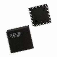
P87C591VFA/00,512 NXP Semiconductors, P87C591VFA/00,512 Datasheet - Page 117

P87C591VFA/00,512
Manufacturer Part Number
P87C591VFA/00,512
Description
IC 80C51 MCU 16K OTP 44-PLCC
Manufacturer
NXP Semiconductors
Series
87Cr
Datasheet
1.P87C591VFA00512.pdf
(160 pages)
Specifications of P87C591VFA/00,512
Core Processor
8051
Core Size
8-Bit
Speed
12MHz
Connectivity
CAN, EBI/EMI, I²C, UART/USART
Peripherals
POR, PWM, WDT
Number Of I /o
32
Program Memory Size
16KB (16K x 8)
Program Memory Type
OTP
Ram Size
512 x 8
Voltage - Supply (vcc/vdd)
4.75 V ~ 5.25 V
Data Converters
A/D 6x10b
Oscillator Type
Internal
Operating Temperature
-40°C ~ 85°C
Package / Case
44-PLCC
Processor Series
P87C5x
Core
80C51
Data Bus Width
8 bit
Data Ram Size
512 B
Interface Type
CAN, I2C, UART
Maximum Clock Frequency
12 MHz
Number Of Programmable I/os
32
Number Of Timers
3
Maximum Operating Temperature
+ 85 C
Mounting Style
SMD/SMT
3rd Party Development Tools
PK51, CA51, A51, ULINK2
Minimum Operating Temperature
- 40 C
On-chip Adc
10 bit, 6 Channel
Lead Free Status / RoHS Status
Lead free / RoHS Compliant
Eeprom Size
-
Lead Free Status / Rohs Status
Details
Other names
568-1256-5
935268182512
P87C591VFAA
935268182512
P87C591VFAA
Available stocks
Company
Part Number
Manufacturer
Quantity
Price
Company:
Part Number:
P87C591VFA/00,512
Manufacturer:
TI
Quantity:
8
Company:
Part Number:
P87C591VFA/00,512
Manufacturer:
NXP Semiconductors
Quantity:
10 000
Philips Semiconductors
16.1.4
The four 16-bit capture registers that Timer T2 is
connected to are: CT0, CT1, CT2, and CT3. These
registers are loaded with the contents of Timer T2, and an
interrupt is requested upon receipt of the input signals
CT0l, CT1I, CT2l, or CT3l. These input signals are shared
with port 1. The four interrupt flags are in the Timer T2
interrupt register (TM2lR special function register). If the
16.1.4.1
Table 72 Capture Control Register (address EBH)
Table 73 Description of CTCON bits
16.1.5
When a recurring external event is represented in the form
of rising or falling edges on one of the four capture pins,
the time between two events can be measured using
Timer T2 and a capture register. When an event occurs,
the contents of Timer T2 are copied into the relevant
capture register and an interrupt request is generated. The
interrupt service routine may then compute the interval
time if it knows the previous contents of Timer T2 when the
last event occurred. With a 6 MHz oscillator, Timer T2 can
be programmed to overflow every 524 ms. When event
interval times are shorter than this, computing the interval
time is simple, and the interrupt service routine is short.
For longer interval times, the Timer T2 extension routine
may be used.
16.1.6
Each time Timer T2 is incremented, the contents of the
three 16-bit compare registers CM0, CM1, and CM2 are
compared with the new counter value of Timer T2. When
a match is found, the corresponding interrupt flag in TM2lR
is set at the end of the following cycle. When a match with
2000 Jul 26
Single-chip 8-bit microcontroller with CAN controller
BIT
7
6
5
4
3
2
1
0
CTN3
7
C
M
C
APTURE
OMPARE
EASURING
Capture Control Register (CTCON)
SYMBOL
CTN3
CTN2
CTN1
CTN0
CTP3
CTP2
CTP1
CTP0
L
L
CTP3
OGIC
OGIC
T
6
IME
I
NTERVALS
Capture Register 3 triggered by a falling edge on CT3l.
Capture Register 3 triggered by a rising edge on CT3l.
Capture Register 2 triggered by a falling edge on CT2l.
Capture Register 2 triggered by a rising edge on CT2l.
Capture Register 1 triggered by a falling edge on CT1l.
Capture Register 1 triggered by a rising edge on CT1l.
Capture Register 0 triggered by a falling edge on CT0l.
Capture Register 0 triggered by a rising edge on CT0l.
CTN2
5
U
SING
R
EGISTERS
CTP2
4
117
capture facility is not required, these inputs can be
regarded as additional external interrupt inputs (INT2 to
INT5).
Using the capture control register CTCON (see
Section 16.1.4.1), these inputs may capture on a rising
edge, a falling edge, or on either a rising or falling edge.
The inputs are sampled during S1P1 of each cycle. When
a selected edge is detected, the contents of Timer T2 are
captured at the end of the cycle.
CM0 occurs, the controller sets bits 0-3 of port 3 if the
corresponding bits of the set enable register STE are at
logic 1 (see Section 16.1.6.2).
When a match with CM1 occurs, the controller resets bits
0-3 of port 3 if the corresponding bits of the reset/enable
register RTE are at logic 1 (see Section 16.1.6.1). If RTE
is “0”, then P3.n is not affected by a match between CM1
or CM2 and Timer 2.
Thus, if the current operation is “set,” the next operation
will be “reset” even if the port latch is reset by software
before the “reset” operation occurs. CM0, CM1, and CM2
are reset by the RST signal.
The modified port latch information appears at the port pin
during S5P1 of the cycle following the cycle in which a
match occurred. If the port is modified by software, the
outputs change during S1P1 of the following cycle. Each
port 3 bit (0-3) can be set or reset by software at any time.
A hardware modification resulting from a comparator
match takes precedence over a software modification in
the same cycle. When the comparator results require a
“set” and a “reset” at the same time, the port latch will be
reset.
CTN1
3
DESCRIPTION
CTP1
2
CTN0
Preliminary Specification
1
P8xC591
CTP0
0


