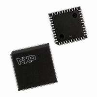
P87C591VFA/00,512 NXP Semiconductors, P87C591VFA/00,512 Datasheet - Page 80

P87C591VFA/00,512
Manufacturer Part Number
P87C591VFA/00,512
Description
IC 80C51 MCU 16K OTP 44-PLCC
Manufacturer
NXP Semiconductors
Series
87Cr
Datasheet
1.P87C591VFA00512.pdf
(160 pages)
Specifications of P87C591VFA/00,512
Core Processor
8051
Core Size
8-Bit
Speed
12MHz
Connectivity
CAN, EBI/EMI, I²C, UART/USART
Peripherals
POR, PWM, WDT
Number Of I /o
32
Program Memory Size
16KB (16K x 8)
Program Memory Type
OTP
Ram Size
512 x 8
Voltage - Supply (vcc/vdd)
4.75 V ~ 5.25 V
Data Converters
A/D 6x10b
Oscillator Type
Internal
Operating Temperature
-40°C ~ 85°C
Package / Case
44-PLCC
Processor Series
P87C5x
Core
80C51
Data Bus Width
8 bit
Data Ram Size
512 B
Interface Type
CAN, I2C, UART
Maximum Clock Frequency
12 MHz
Number Of Programmable I/os
32
Number Of Timers
3
Maximum Operating Temperature
+ 85 C
Mounting Style
SMD/SMT
3rd Party Development Tools
PK51, CA51, A51, ULINK2
Minimum Operating Temperature
- 40 C
On-chip Adc
10 bit, 6 Channel
Lead Free Status / RoHS Status
Lead free / RoHS Compliant
Eeprom Size
-
Lead Free Status / Rohs Status
Details
Other names
568-1256-5
935268182512
P87C591VFAA
935268182512
P87C591VFAA
Available stocks
Company
Part Number
Manufacturer
Quantity
Price
Company:
Part Number:
P87C591VFA/00,512
Manufacturer:
TI
Quantity:
8
Company:
Part Number:
P87C591VFA/00,512
Manufacturer:
NXP Semiconductors
Quantity:
10 000
Philips Semiconductors
15.2.10.1 The Address Register, S1ADR
The CPU can read from and write to this 8-bit, directly
addressable SFR. S1ADR is not affected by the SIO1
hardware. The contents of this register are irrelevant when
SIO1 is in a master mode. In the slave modes, the seven
most significant bits must be loaded with the
microcontrollers own slave address, and, if the least
Table 51 Address Register S1ADR (address DBH)
Table 52 Description of S1ADR (DBH) bits
15.2.11 T
S1DAT contains a byte of serial data to be transmitted or
a byte which has just been received. The CPU can read
from and write to this 8-bit, directly addressable SFR while
it is not in the process of shifting a byte. This occurs when
SIO1 is in a defined state and the serial interrupt flag is set.
Data in S1DAT remains stable as long as SI is set. Data in
S1DAT is always shifted from right to left: the first bit to be
transmitted is the MSB (bit 7), and, after a byte has been
received, the first bit of received data is located at the MSB
of S1DAT. While data is being shifted out, data on the bus
is simultaneously being shifted in; S1DAT always contains
the last data byte present on the bus. Thus, in the event of
lost arbitration, the transition from master transmitter to
slave receiver is made with the correct data in S1DAT.
S1DAT and the ACK flag form a 9-bit shift register which
shifts in or shifts out an 8-bit byte, followed by an
Table 53 Address Register S1DAT (address DAH)
Table 54 Description of S1DAT (DAH) bits
2000 Jul 26
Single-chip 8-bit microcontroller with CAN controller
7 to 1
7 to 0
BIT
BIT
SD7
0
X
7
7
HE
D
ATA
SD7 to SD0
SYMBOL
SYMBOL
R
GC
SD6
EGISTER
X
X
6
6
, S1DAT
Own slave address.
0 = general call address is not recognized.
1 = general call address is recognized.
Eight bits to be transmitted or just received. A logic 1 in S1DAT corresponds to a high
level on the I
shifts through S1DAT from right to left. Figure 35 shows how data in S1DAT is serially
transferred to and from the SDA line.
SD5
X
5
5
2
C bus, and a logic 0 corresponds to a low level on the bus. Serial data
SD4
X
4
4
80
significant bit is set, the general call address (00H) is
recognized; otherwise it is ignored.
The most significant bit corresponds to the first bit received
from the I
corresponds to a high level on the I
corresponds to a low level on the bus.
acknowledge bit. The ACK flag is controlled by the SIO1
hardware and cannot be accessed by the CPU. Serial data
is shifted through the ACK flag into S1DAT on the rising
edges of serial clock pulses on the SCL line. When a byte
has been shifted into S1DAT, the serial data is available in
S1DAT, and the acknowledge bit is returned by the control
logic during the ninth clock pulse. Serial data is shifted out
from S1DAT via a buffer (BSD7) on the falling edges of
clock pulses on the SCL line.
When the CPU writes to S1DAT, BSD7 is loaded with the
content of S1DAT.7, which is the first bit to be transmitted
to the SDA line (see Figure 36). After nine serial clock
pulses, the eight bits in S1DAT will have been transmitted
to the SDA line, and the acknowledge bit will be present in
ACK. Note that the eight transmitted bits are shifted back
into S1DAT.
SD3
X
3
3
DESCRIPTION
DESCRIPTION
2
C bus after a start condition. A logic 1 in S1ADR
SD2
X
2
2
Preliminary Specification
SD1
X
1
1
2
C bus, and a logic 0
P8xC591
SD0
GC
0
0


