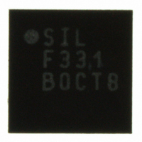
C8051F331-GM Silicon Laboratories Inc, C8051F331-GM Datasheet - Page 37

C8051F331-GM
Manufacturer Part Number
C8051F331-GM
Description
IC 8051 MCU 8K FLASH 20QFN
Manufacturer
Silicon Laboratories Inc
Series
C8051F33xr
Specifications of C8051F331-GM
Program Memory Type
FLASH
Program Memory Size
8KB (8K x 8)
Package / Case
20-QFN
Core Processor
8051
Core Size
8-Bit
Speed
25MHz
Connectivity
SMBus (2-Wire/I²C), SPI, UART/USART
Peripherals
POR, PWM, WDT
Number Of I /o
17
Ram Size
768 x 8
Voltage - Supply (vcc/vdd)
2.7 V ~ 3.6 V
Oscillator Type
Internal
Operating Temperature
-40°C ~ 85°C
Processor Series
C8051F3x
Core
8051
Data Bus Width
8 bit
Data Ram Size
768 B
Interface Type
I2C/SMBus/SPI/UART
Maximum Clock Frequency
25 MHz
Number Of Programmable I/os
17
Number Of Timers
4
Operating Supply Voltage
2.7 V to 3.6 V
Maximum Operating Temperature
+ 85 C
Mounting Style
SMD/SMT
3rd Party Development Tools
KSK-SL-TOOLSTICK, PK51, CA51, A51, ULINK2
Development Tools By Supplier
C8051F330DK
Minimum Operating Temperature
- 40 C
On-chip Adc
10 bit, 16 Channel
No. Of I/o's
17
Ram Memory Size
768Byte
Cpu Speed
25MHz
No. Of Timers
4
Rohs Compliant
Yes
Lead Free Status / RoHS Status
Lead free / RoHS Compliant
For Use With
770-1006 - ISP 4PORT FOR SILABS C8051F MCU336-1451 - ADAPTER PROGRAM TOOLSTICK F330336-1264 - DEV KIT FOR C8051F330/F331
Eeprom Size
-
Data Converters
-
Lead Free Status / Rohs Status
Lead free / RoHS Compliant
Other names
336-1265
Available stocks
Company
Part Number
Manufacturer
Quantity
Price
Company:
Part Number:
C8051F331-GM
Manufacturer:
SiliconL
Quantity:
1 630
Part Number:
C8051F331-GM
Manufacturer:
SILICON LABS/èٹ¯ç§‘
Quantity:
20 000
Part Number:
C8051F331-GMR
Manufacturer:
SILICON LABS/èٹ¯ç§‘
Quantity:
20 000
Notes:
General
Solder Mask Design
Stencil Design
Card Assembly
Dimension
1. All dimensions shown are in millimeters (mm) unless otherwise noted.
2. Dimensioning and Tolerancing is per the ANSI Y14.5M-1994 specification.
3. This Land Pattern Design is based on the IPC-7351 guidelines.
4. All metal pads are to be non-solder mask defined (NSMD). Clearance between the solder
5. A stainless steel, laser-cut and electro-polished stencil with trapezoidal walls should be used
6. The stencil thickness should be 0.125 mm (5 mils).
7. The ratio of stencil aperture to land pad size should be 1:1 for all perimeter pins.
8. A 2x2 array of 0.95 mm openings on a 1.1 mm pitch should be used for the center pad to
9. A No-Clean, Type-3 solder paste is recommended.
10. The recommended card reflow profile is per the JEDEC/IPC J-STD-020 specification for Small
C1
C2
X1
E
mask and the metal pad is to be 60 m minimum, all the way around the pad.
to assure good solder paste release.
assure the proper paste volume (71% Paste Coverage).
Body Components.
Figure 4.3. QFN-20 Recommended PCB Land Pattern
Table 4.3. QFN-20 PCB Land Pattern Dimesions
0.20
Min
3.70
3.70
0.50
Max
0.30
Rev. 1.7
Dimension
X2
Y1
Y2
C8051F330/1/2/3/4/5
2.15
0.90
2.15
Min
Max
2.25
1.00
2.25
39


