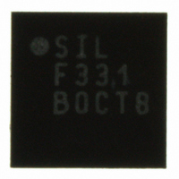
C8051F331-GM Silicon Laboratories Inc, C8051F331-GM Datasheet - Page 42

C8051F331-GM
Manufacturer Part Number
C8051F331-GM
Description
IC 8051 MCU 8K FLASH 20QFN
Manufacturer
Silicon Laboratories Inc
Series
C8051F33xr
Specifications of C8051F331-GM
Program Memory Type
FLASH
Program Memory Size
8KB (8K x 8)
Package / Case
20-QFN
Core Processor
8051
Core Size
8-Bit
Speed
25MHz
Connectivity
SMBus (2-Wire/I²C), SPI, UART/USART
Peripherals
POR, PWM, WDT
Number Of I /o
17
Ram Size
768 x 8
Voltage - Supply (vcc/vdd)
2.7 V ~ 3.6 V
Oscillator Type
Internal
Operating Temperature
-40°C ~ 85°C
Processor Series
C8051F3x
Core
8051
Data Bus Width
8 bit
Data Ram Size
768 B
Interface Type
I2C/SMBus/SPI/UART
Maximum Clock Frequency
25 MHz
Number Of Programmable I/os
17
Number Of Timers
4
Operating Supply Voltage
2.7 V to 3.6 V
Maximum Operating Temperature
+ 85 C
Mounting Style
SMD/SMT
3rd Party Development Tools
KSK-SL-TOOLSTICK, PK51, CA51, A51, ULINK2
Development Tools By Supplier
C8051F330DK
Minimum Operating Temperature
- 40 C
On-chip Adc
10 bit, 16 Channel
No. Of I/o's
17
Ram Memory Size
768Byte
Cpu Speed
25MHz
No. Of Timers
4
Rohs Compliant
Yes
Lead Free Status / RoHS Status
Lead free / RoHS Compliant
For Use With
770-1006 - ISP 4PORT FOR SILABS C8051F MCU336-1451 - ADAPTER PROGRAM TOOLSTICK F330336-1264 - DEV KIT FOR C8051F330/F331
Eeprom Size
-
Data Converters
-
Lead Free Status / Rohs Status
Lead free / RoHS Compliant
Other names
336-1265
Available stocks
Company
Part Number
Manufacturer
Quantity
Price
Company:
Part Number:
C8051F331-GM
Manufacturer:
SiliconL
Quantity:
1 630
Part Number:
C8051F331-GM
Manufacturer:
SILICON LABS/èٹ¯ç§‘
Quantity:
20 000
Part Number:
C8051F331-GMR
Manufacturer:
SILICON LABS/èٹ¯ç§‘
Quantity:
20 000
5.3.2. Tracking Modes
Each ADC0 conversion must be preceded by a minimum tracking time in order for the converted result to
be accurate. The minimum tracking time is given in Table 5.1. The AD0TM bit in register ADC0CN controls
the ADC0 track-and-hold mode. In its default state, the ADC0 input is continuously tracked, except when a
conversion is in progress. When the AD0TM bit is logic 1, ADC0 operates in low-power track-and-hold
mode. In this mode, each conversion is preceded by a tracking period of 3 SAR clocks (after the start-of-
conversion signal). When the CNVSTR signal is used to initiate conversions in low-power tracking mode,
ADC0 tracks only when CNVSTR is low; conversion begins on the rising edge of CNVSTR (see
Figure 5.3). Tracking can also be disabled (shutdown) when the device is in low power standby or sleep
modes. Low-power track-and-hold mode is also useful when AMUX settings are frequently changed, due
to the settling time requirements described in
(AD0CM[2:0]=000, 001,010
Timer 1, Timer 3 Overflow
Write '1' to AD0BUSY,
(AD0CM[2:0]=100)
Timer 0, Timer 2,
Figure 5.3. 10-Bit ADC Track and Conversion Example Timing
SAR Clocks
SAR Clocks
SAR Clocks
AD0TM=1
AD0TM=0
011, 101)
AD0TM=1
AD0TM=0
CNVSTR
Low Power
or Convert
Low Power
or Convert
Track or
Convert
A. ADC0 Timing for External Trigger Source
Track or Convert
B. ADC0 Timing for Internal Trigger Source
1
1
Section “5.3.3. Settling Time Requirements” on page
Track
2
2
Track
Rev. 1.7
3
3
4
4
1
5
5
Convert
2
6
6
3
7
7
C8051F330/1/2/3/4/5
4
8
Convert
8
Convert
Convert
5
9
9
6
10 11 12
10 11
7
8
9
13 14
10 11
Low Power Mode
Track
Low Power
Mode
Track
46.
45


