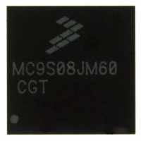
MC9S08JM60CGT Freescale Semiconductor, MC9S08JM60CGT Datasheet - Page 197

MC9S08JM60CGT
Manufacturer Part Number
MC9S08JM60CGT
Description
IC MCU 8BIT 60K FLASH 48-QFN
Manufacturer
Freescale Semiconductor
Series
HCS08r
Datasheet
1.MC9S08JM32CLD.pdf
(388 pages)
Specifications of MC9S08JM60CGT
Core Processor
HCS08
Core Size
8-Bit
Speed
48MHz
Connectivity
I²C, LIN, SCI, SPI, USB
Peripherals
LVD, POR, PWM, WDT
Number Of I /o
37
Program Memory Size
60KB (60K x 8)
Program Memory Type
FLASH
Ram Size
4K x 8
Voltage - Supply (vcc/vdd)
2.7 V ~ 5.5 V
Data Converters
A/D 8x12b
Oscillator Type
External
Operating Temperature
-40°C ~ 85°C
Package / Case
48-QFN
Processor Series
S08JM
Core
HCS08
Data Bus Width
8 bit
Data Ram Size
4 KB
Interface Type
SCI/SPI
Maximum Clock Frequency
24 MHz
Number Of Programmable I/os
37
Number Of Timers
8
Maximum Operating Temperature
+ 85 C
Mounting Style
SMD/SMT
3rd Party Development Tools
EWS08
Development Tools By Supplier
DEMOJM, DEMOJMSKT, DEMOFLEXISJMSD, DEMO9S08JM16
Minimum Operating Temperature
- 40 C
On-chip Adc
8-ch x 12-bit
Cpu Family
HCS08
Device Core Size
8b
Frequency (max)
24MHz
Total Internal Ram Size
4KB
# I/os (max)
37
Number Of Timers - General Purpose
8
Operating Supply Voltage (typ)
3.3/5V
Operating Supply Voltage (max)
5.5V
Operating Supply Voltage (min)
2.7V
Instruction Set Architecture
CISC
Operating Temp Range
-40C to 85C
Operating Temperature Classification
Industrial
Mounting
Surface Mount
Pin Count
48
Package Type
QFN EP
Package
48QFN EP
Family Name
HCS08
Maximum Speed
24 MHz
Operating Supply Voltage
3.3|5 V
For Use With
DEMOJM - KIT DEMO FOR JM MCU FAMILYDEMOJMSKT - BOARD DEMO S08JM CARD W/SOCKET
Lead Free Status / RoHS Status
Lead free / RoHS Compliant
Eeprom Size
-
Lead Free Status / Rohs Status
Lead free / RoHS Compliant
Available stocks
Company
Part Number
Manufacturer
Quantity
Price
- Current page: 197 of 388
- Download datasheet (5Mb)
12.4.4
The low power bit (LP) is provided to allow the FLL or PLL to be disabled and thus conserve power when
these systems are not being used. However, in some applications it may be desirable to enable the FLL or
PLL and allow it to lock for maximum accuracy before switching to an engaged mode. Do this by writing
the LP bit to 0.
12.4.5
When IRCLKEN is set the internal reference clock signal will be presented as MCGIRCLK, which can be
used as an additional clock source. The MCGIRCLK frequency can be re-targeted by trimming the period
of the internal reference clock. This can be done by writing a new value to the TRIM bits in the MCGTRM
register. Writing a larger value will decrease the MCGIRCLK frequency, and writing a smaller value to
the MCGTRM register will increase the MCGIRCLK frequency. The TRIM bits will effect the MCGOUT
frequency if the MCG is in FLL engaged internal (FEI), FLL bypassed internal (FBI), or bypassed low
power internal (BLPI) mode. The TRIM and FTRIM value is initialized by POR but is not affected by
other resets.
Until MCGIRCLK is trimmed, programming low reference divider (RDIV) factors may result in
MCGOUT frequencies that exceed the maximum chip-level frequency and violate the chip-level clock
timing specifications (see the
If IREFSTEN and IRCLKEN bits are both set, the internal reference clock will keep running during stop
mode in order to provide a fast recovery upon exiting stop.
12.4.6
The MCG module can support an external reference clock with frequencies between 31.25 kHz to 5 MHz
in FEE and FBE modes, 1 MHz to 16 MHz in PEE and PBE modes, and 0 to 40 MHz in BLPE mode.
When ERCLKEN is set, the external reference clock signal will be presented as MCGERCLK, which can
be used as an additional clock source. When IREFS = 1, the external reference clock will not be used by
the FLL or PLL and will only be used as MCGERCLK. In these modes, the frequency can be equal to the
maximum frequency the chip-level timing specifications will support (see the
If EREFSTEN and ERCLKEN bits are both set or the MCG is in FEE, FBE, PEE, PBE or BLPE mode,
the external reference clock will keep running during stop mode in order to provide a fast recovery upon
exiting stop.
If CME bit is written to 1, the clock monitor is enabled. If the external reference falls below a certain
frequency (f
LOC bit in the System Reset Status (SRS) register will be set to indicate the error.
12.4.7
The MCG presents the divided reference clock as MCGFFCLK for use as an additional clock source. The
MCGFFCLK frequency must be no more than 1/4 of the MCGOUT frequency to be valid. Because of this
requirement, the MCGFFCLK is not valid in bypass modes for the following combinations of BDIV and
RDIV values:
Freescale Semiconductor
Low Power Bit Usage
Internal Reference Clock
External Reference Clock
Fixed Frequency Clock
loc_high
or f
loc_low
Device Overview
depending on the RANGE bit in the MCGC2), the MCU will reset. The
MC9S08JM60 Series Data Sheet, Rev. 3
chapter).
Multi-Purpose Clock Generator (S08MCGV1)
Device Overview
chapter).
197
Related parts for MC9S08JM60CGT
Image
Part Number
Description
Manufacturer
Datasheet
Request
R
Part Number:
Description:
Manufacturer:
Freescale Semiconductor, Inc
Datasheet:
Part Number:
Description:
Manufacturer:
Freescale Semiconductor, Inc
Datasheet:
Part Number:
Description:
Manufacturer:
Freescale Semiconductor, Inc
Datasheet:
Part Number:
Description:
Manufacturer:
Freescale Semiconductor, Inc
Datasheet:
Part Number:
Description:
Manufacturer:
Freescale Semiconductor, Inc
Datasheet:
Part Number:
Description:
Manufacturer:
Freescale Semiconductor, Inc
Datasheet:
Part Number:
Description:
Manufacturer:
Freescale Semiconductor, Inc
Datasheet:
Part Number:
Description:
Manufacturer:
Freescale Semiconductor, Inc
Datasheet:
Part Number:
Description:
Manufacturer:
Freescale Semiconductor, Inc
Datasheet:
Part Number:
Description:
Manufacturer:
Freescale Semiconductor, Inc
Datasheet:
Part Number:
Description:
Manufacturer:
Freescale Semiconductor, Inc
Datasheet:
Part Number:
Description:
Manufacturer:
Freescale Semiconductor, Inc
Datasheet:
Part Number:
Description:
Manufacturer:
Freescale Semiconductor, Inc
Datasheet:
Part Number:
Description:
Manufacturer:
Freescale Semiconductor, Inc
Datasheet:
Part Number:
Description:
Manufacturer:
Freescale Semiconductor, Inc
Datasheet:


