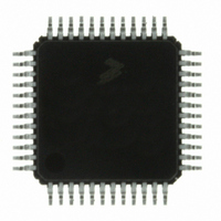
MC9S08DZ60ACLF Freescale Semiconductor, MC9S08DZ60ACLF Datasheet - Page 191

MC9S08DZ60ACLF
Manufacturer Part Number
MC9S08DZ60ACLF
Description
IC MCU 60K FLASH 4K RAM 48-LQFP
Manufacturer
Freescale Semiconductor
Series
HCS08r
Datasheets
1.DEMO9S08DZ60.pdf
(416 pages)
2.EVB9S08DZ60.pdf
(4 pages)
3.MC9S08DZ48AMLF.pdf
(458 pages)
Specifications of MC9S08DZ60ACLF
Core Processor
HCS08
Core Size
8-Bit
Speed
40MHz
Connectivity
CAN, I²C, LIN, SCI, SPI
Peripherals
LVD, POR, PWM, WDT
Number Of I /o
39
Program Memory Size
60KB (60K x 8)
Program Memory Type
FLASH
Eeprom Size
2K x 8
Ram Size
4K x 8
Voltage - Supply (vcc/vdd)
2.7 V ~ 5.5 V
Data Converters
A/D 16x12b
Oscillator Type
External
Operating Temperature
-40°C ~ 85°C
Package / Case
48-LQFP
Processor Series
S08DZ
Core
HCS08
Data Bus Width
8 bit
Data Ram Size
4 KB
Interface Type
CAN, I2C, SCI, SPI
Maximum Clock Frequency
40 MHz
Number Of Programmable I/os
53
Number Of Timers
2
Operating Supply Voltage
5.5 V
Maximum Operating Temperature
+ 85 C
Mounting Style
SMD/SMT
3rd Party Development Tools
EWS08
Development Tools By Supplier
DEMO9S08DZ60
Minimum Operating Temperature
- 40 C
On-chip Adc
12 bit, 24 Channel
For Use With
DEMO9S08DZ60 - BOARD DEMOEVB9S08DZ60 - BOARD EVAL FOR 9S08DZ60
Lead Free Status / RoHS Status
Lead free / RoHS Compliant
Available stocks
Company
Part Number
Manufacturer
Quantity
Price
Company:
Part Number:
MC9S08DZ60ACLF
Manufacturer:
FREESCAL
Quantity:
1 250
Company:
Part Number:
MC9S08DZ60ACLF
Manufacturer:
Freescale Semiconductor
Quantity:
10 000
- Current page: 191 of 458
- Download datasheet (5Mb)
8.5.3.2
In this example, the MCG will move through the proper operational modes from PEE mode with an 8MHz
crystal configured for an 16 MHz bus frequency (see previous example) to BLPI mode with a 16 kHz bus
frequency.First, the code sequence will be described. Then a flowchart will be included which illustrates
the sequence.
Freescale Semiconductor
1. First, PEE must transition to PBE mode:
2. Then, PBE must transition either directly to FBE mode or first through BLPE mode and then to
3. Next, FBE mode transitions into FBI mode:
a) MCGC1 = 0x98 (%10011000)
b) Loop until CLKST (bits 3 and 2) in MCGSC are %10, indicating that the external reference
FBE mode:
a) BLPE: If a transition through BLPE mode is desired, first set LP (bit 3) in MCGC2 to 1
b) BLPE/FBE: MCGC3 = 0x18(%00011000)
c) BLPE: If transitioning through BLPE mode, clear LP (bit 3) in MCGC2 to 0 here to switch to
d) FBE: Loop until PLLST (bit 5) in MCGSC is clear, indicating that the current source for the
e) FBE: Optionally, loop until LOCK (bit 6) in the MCGSC is set, indicating that the FLL has
a) MCGC1 = 0x5C (%01011100)
– CLKS (bits 7 and 6) set to %10 in order to switch the system clock source to the external
clock is selected to feed MCGOUT
– PLLS (bit 6) clear to 0 to select the FLL. At this time, with an RDIV value of %011, the PLL
– DIV32 (bit 4) set to 1 (if previously cleared), automatically switches RDIV bits to the proper
FBE mode
PLLS clock is the FLL
acquired lock. Although the FLL is bypassed in FBE mode, it is still enabled and running.
– CLKS (bits7 and 6) in MCGSC1 set to %01 in order to switch the system clock to the
Example # 2: Moving from PEE to BLPI Mode: Bus Frequency =16 kHz
reference clock
reference divider of 8 is switched to an FLL divider of 256 (see
reference frequency of 8 MHz / 256 = 31.25 kHz. If RDIV was not previously set to %011
(necessary to achieve required 31.25-39.06 kHz FLL reference frequency with an 8 MHz
external source frequency), it must be changed prior to clearing the PLLS bit. In BLPE
mode,changing this bit only prepares the MCG for FLL usage in FBE mode. With PLLS =
0, the VDIV value does not matter.
reference divider for the FLL clock (divide-by-256)
internal reference clock
MC9S08DZ128 Series Data Sheet, Rev. 1
Chapter 8 Multi-Purpose Clock Generator (S08MCGV2)
Table
8-2), resulting in a
191
Related parts for MC9S08DZ60ACLF
Image
Part Number
Description
Manufacturer
Datasheet
Request
R
Part Number:
Description:
Manufacturer:
Freescale Semiconductor, Inc
Datasheet:
Part Number:
Description:
Manufacturer:
Freescale Semiconductor, Inc
Datasheet:
Part Number:
Description:
Manufacturer:
Freescale Semiconductor, Inc
Datasheet:
Part Number:
Description:
Manufacturer:
Freescale Semiconductor, Inc
Datasheet:
Part Number:
Description:
Manufacturer:
Freescale Semiconductor, Inc
Datasheet:
Part Number:
Description:
Manufacturer:
Freescale Semiconductor, Inc
Datasheet:
Part Number:
Description:
Manufacturer:
Freescale Semiconductor, Inc
Datasheet:
Part Number:
Description:
Manufacturer:
Freescale Semiconductor, Inc
Datasheet:
Part Number:
Description:
Manufacturer:
Freescale Semiconductor, Inc
Datasheet:
Part Number:
Description:
Manufacturer:
Freescale Semiconductor, Inc
Datasheet:
Part Number:
Description:
Manufacturer:
Freescale Semiconductor, Inc
Datasheet:
Part Number:
Description:
Manufacturer:
Freescale Semiconductor, Inc
Datasheet:
Part Number:
Description:
Manufacturer:
Freescale Semiconductor, Inc
Datasheet:
Part Number:
Description:
Manufacturer:
Freescale Semiconductor, Inc
Datasheet:
Part Number:
Description:
Manufacturer:
Freescale Semiconductor, Inc
Datasheet:


