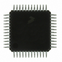
MC9S08DZ60ACLF Freescale Semiconductor, MC9S08DZ60ACLF Datasheet - Page 61

MC9S08DZ60ACLF
Manufacturer Part Number
MC9S08DZ60ACLF
Description
IC MCU 60K FLASH 4K RAM 48-LQFP
Manufacturer
Freescale Semiconductor
Series
HCS08r
Datasheets
1.DEMO9S08DZ60.pdf
(416 pages)
2.EVB9S08DZ60.pdf
(4 pages)
3.MC9S08DZ48AMLF.pdf
(458 pages)
Specifications of MC9S08DZ60ACLF
Core Processor
HCS08
Core Size
8-Bit
Speed
40MHz
Connectivity
CAN, I²C, LIN, SCI, SPI
Peripherals
LVD, POR, PWM, WDT
Number Of I /o
39
Program Memory Size
60KB (60K x 8)
Program Memory Type
FLASH
Eeprom Size
2K x 8
Ram Size
4K x 8
Voltage - Supply (vcc/vdd)
2.7 V ~ 5.5 V
Data Converters
A/D 16x12b
Oscillator Type
External
Operating Temperature
-40°C ~ 85°C
Package / Case
48-LQFP
Processor Series
S08DZ
Core
HCS08
Data Bus Width
8 bit
Data Ram Size
4 KB
Interface Type
CAN, I2C, SCI, SPI
Maximum Clock Frequency
40 MHz
Number Of Programmable I/os
53
Number Of Timers
2
Operating Supply Voltage
5.5 V
Maximum Operating Temperature
+ 85 C
Mounting Style
SMD/SMT
3rd Party Development Tools
EWS08
Development Tools By Supplier
DEMO9S08DZ60
Minimum Operating Temperature
- 40 C
On-chip Adc
12 bit, 24 Channel
For Use With
DEMO9S08DZ60 - BOARD DEMOEVB9S08DZ60 - BOARD EVAL FOR 9S08DZ60
Lead Free Status / RoHS Status
Lead free / RoHS Compliant
Available stocks
Company
Part Number
Manufacturer
Quantity
Price
Company:
Part Number:
MC9S08DZ60ACLF
Manufacturer:
FREESCAL
Quantity:
1 250
Company:
Part Number:
MC9S08DZ60ACLF
Manufacturer:
Freescale Semiconductor
Quantity:
10 000
- Current page: 61 of 458
- Download datasheet (5Mb)
debug interface) and verifying that FLASH is blank. To avoid returning to secure mode after the next reset,
program the security bits (SEC) to the unsecured state (1:0).
4.4
The memory management unit (MMU) allows the program and data space for the HCS08 Family of
Microcontrollers to be extended beyond the 64K CPU addressable memory map. The extended memory
when used for data can also be accessed linearly using a linear address pointer and data access registers.
4.4.1
Key features of the MMU module are:
4.4.2
The HCS08 Core architecture limits the CPU addressable space available to 64K bytes. The Program Page
(PPAGE) allows for integrating up to 128K of FLASH into the system by selecting one of the 16K byte
blocks to be accessed through the Paging Window located at 0x8000-0xBFFF. The MMU module also
provides a linear address pointer that allows extension of data access up to 128K.
4.4.2.1
The PPAGE register holds the page select value for the Paging Window. The value in PPAGE can be
manipulated by using normal read and write instructions as well as the CALL and RTC instructions. The
user should not change PPAGE directly when running from paged memory, only CALL and RTC should
be used.
Freescale Semiconductor
•
•
•
Memory Management Unit extends the HCS08 memory space
— up to 128K for program and data space
Extended program space using paging scheme
— PPAGE register used for page selection
— fixed 16K byte memory window
— architecture supports eight 16K pages
Extended data space using linear address pointer
— 17-bit linear address pointer
— linear address pointer and data register provided in direct page allows access of complete
— optional auto increment of pointer when data accessed
— supports a 2s complement addition/subtraction to address pointer without using any math
— supports word accesses to any address specified by the linear address pointer when using
Memory Management Unit
FLASH memory map using direct page instructions
instructions or memory resources
LDHX, STHX instructions
Features
Memory Expansion
Program Space
MC9S08DZ128 Series Data Sheet, Rev. 1
Chapter 4 Memory
61
Related parts for MC9S08DZ60ACLF
Image
Part Number
Description
Manufacturer
Datasheet
Request
R
Part Number:
Description:
Manufacturer:
Freescale Semiconductor, Inc
Datasheet:
Part Number:
Description:
Manufacturer:
Freescale Semiconductor, Inc
Datasheet:
Part Number:
Description:
Manufacturer:
Freescale Semiconductor, Inc
Datasheet:
Part Number:
Description:
Manufacturer:
Freescale Semiconductor, Inc
Datasheet:
Part Number:
Description:
Manufacturer:
Freescale Semiconductor, Inc
Datasheet:
Part Number:
Description:
Manufacturer:
Freescale Semiconductor, Inc
Datasheet:
Part Number:
Description:
Manufacturer:
Freescale Semiconductor, Inc
Datasheet:
Part Number:
Description:
Manufacturer:
Freescale Semiconductor, Inc
Datasheet:
Part Number:
Description:
Manufacturer:
Freescale Semiconductor, Inc
Datasheet:
Part Number:
Description:
Manufacturer:
Freescale Semiconductor, Inc
Datasheet:
Part Number:
Description:
Manufacturer:
Freescale Semiconductor, Inc
Datasheet:
Part Number:
Description:
Manufacturer:
Freescale Semiconductor, Inc
Datasheet:
Part Number:
Description:
Manufacturer:
Freescale Semiconductor, Inc
Datasheet:
Part Number:
Description:
Manufacturer:
Freescale Semiconductor, Inc
Datasheet:
Part Number:
Description:
Manufacturer:
Freescale Semiconductor, Inc
Datasheet:


