MC9S08DZ60ACLF Freescale Semiconductor, MC9S08DZ60ACLF Datasheet - Page 406
MC9S08DZ60ACLF
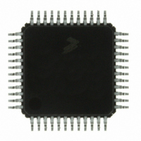
Manufacturer Part Number
MC9S08DZ60ACLF
Description
IC MCU 60K FLASH 4K RAM 48-LQFP
Manufacturer
Freescale Semiconductor
Series
HCS08r
Datasheets
1.DEMO9S08DZ60.pdf
(416 pages)
2.EVB9S08DZ60.pdf
(4 pages)
3.MC9S08DZ48AMLF.pdf
(458 pages)
Specifications of MC9S08DZ60ACLF
Core Processor
HCS08
Core Size
8-Bit
Speed
40MHz
Connectivity
CAN, I²C, LIN, SCI, SPI
Peripherals
LVD, POR, PWM, WDT
Number Of I /o
39
Program Memory Size
60KB (60K x 8)
Program Memory Type
FLASH
Eeprom Size
2K x 8
Ram Size
4K x 8
Voltage - Supply (vcc/vdd)
2.7 V ~ 5.5 V
Data Converters
A/D 16x12b
Oscillator Type
External
Operating Temperature
-40°C ~ 85°C
Package / Case
48-LQFP
Processor Series
S08DZ
Core
HCS08
Data Bus Width
8 bit
Data Ram Size
4 KB
Interface Type
CAN, I2C, SCI, SPI
Maximum Clock Frequency
40 MHz
Number Of Programmable I/os
53
Number Of Timers
2
Operating Supply Voltage
5.5 V
Maximum Operating Temperature
+ 85 C
Mounting Style
SMD/SMT
3rd Party Development Tools
EWS08
Development Tools By Supplier
DEMO9S08DZ60
Minimum Operating Temperature
- 40 C
On-chip Adc
12 bit, 24 Channel
For Use With
DEMO9S08DZ60 - BOARD DEMOEVB9S08DZ60 - BOARD EVAL FOR 9S08DZ60
Lead Free Status / RoHS Status
Lead free / RoHS Compliant
Available stocks
Company
Part Number
Manufacturer
Quantity
Price
Company:

Part Number:
MC9S08DZ60ACLF
Manufacturer:
FREESCAL
Quantity:
1 250
Company:
Part Number:
MC9S08DZ60ACLF
Manufacturer:
Freescale Semiconductor
Quantity:
10 000


Chapter 18 Debug Module (S08DBGV3) (128K)
18.3.3.13 Debug Control Register (DBGC)
1
406
end-run
Module Base + 0x000C
end-run
or non-
In the case of an end-trace to reset where DBGEN=1 and BEGIN=0, the ARM and BRKEN bits are cleared but the remaining
control bits in this register do not change after reset.
DBGEN
BRKEN
LOOP1
Reset
Field
ARM
POR
TAG
7
6
5
4
0
W
R
1
DBGEN
DBG Module Enable Bit — The DBGEN bit enables the DBG module. The DBGEN bit is forced to zero and
cannot be set if the MCU is secure.
0 DBG not enabled
1 DBG enabled
Arm Bit — The ARM bit controls whether the debugger is comparing and storing data in FIFO. See
Section 18.4.4.2, “Arming the DBG Module”
0 Debugger not armed
1 Debugger armed
Tag or Force Bit — The TAG bit controls whether a debugger or comparator C breakpoint will be requested as
a tag or force breakpoint to the CPU. The TAG bit is not used if BRKEN = 0.
0 Force request selected
1 Tag request selected
Break Enable Bit — The BRKEN bit controls whether the debugger will request a breakpoint to the CPU at the
end of a trace run, and whether comparator C will request a breakpoint to the CPU.
0 CPU break request not enabled
1 CPU break request enabled
Select LOOP1 Capture Mode — This bit selects either normal capture mode or LOOP1 capture mode. LOOP1
is not used in event-only modes.
0 Normal operation - capture COF events into the capture buffer FIFO
1 LOOP1 capture mode enabled. When the conditions are met to store a COF value into the FIFO, compare the
U
1
7
current COF address with the address in comparator C. If these addresses match, override the FIFO capture
and do not increment the FIFO count. If the address does not match comparator C, capture the COF address,
including the PPACC indicator, into the FIFO and into comparator C.
= Unimplemented or Reserved
ARM
1
0
6
Figure 18-14. Debug Control Register (DBGC)
Table 18-15. DBGC Field Descriptions
MC9S08DZ128 Series Data Sheet, Rev. 1
TAG
U
0
5
BRKEN
for more information.
0
0
4
Description
0
0
0
3
0
0
0
2
Freescale Semiconductor
0
0
0
1
LOOP1
U
0
0
Related parts for MC9S08DZ60ACLF
Image
Part Number
Description
Manufacturer
Datasheet
Request
R

Part Number:
Description:
Manufacturer:
Freescale Semiconductor, Inc
Datasheet:
Part Number:
Description:
Manufacturer:
Freescale Semiconductor, Inc
Datasheet:
Part Number:
Description:
Manufacturer:
Freescale Semiconductor, Inc
Datasheet:
Part Number:
Description:
Manufacturer:
Freescale Semiconductor, Inc
Datasheet:
Part Number:
Description:
Manufacturer:
Freescale Semiconductor, Inc
Datasheet:
Part Number:
Description:
Manufacturer:
Freescale Semiconductor, Inc
Datasheet:
Part Number:
Description:
Manufacturer:
Freescale Semiconductor, Inc
Datasheet:
Part Number:
Description:
Manufacturer:
Freescale Semiconductor, Inc
Datasheet:
Part Number:
Description:
Manufacturer:
Freescale Semiconductor, Inc
Datasheet:
Part Number:
Description:
Manufacturer:
Freescale Semiconductor, Inc
Datasheet:
Part Number:
Description:
Manufacturer:
Freescale Semiconductor, Inc
Datasheet:
Part Number:
Description:
Manufacturer:
Freescale Semiconductor, Inc
Datasheet:
Part Number:
Description:
Manufacturer:
Freescale Semiconductor, Inc
Datasheet:
Part Number:
Description:
Manufacturer:
Freescale Semiconductor, Inc
Datasheet:
Part Number:
Description:
Manufacturer:
Freescale Semiconductor, Inc
Datasheet: