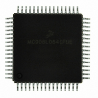
MC908LD64IFUE Freescale Semiconductor, MC908LD64IFUE Datasheet - Page 64

MC908LD64IFUE
Manufacturer Part Number
MC908LD64IFUE
Description
IC MCU 8BIT FOR LCD 64-QFP
Manufacturer
Freescale Semiconductor
Series
HC08r
Datasheet
1.MC908LD64IFUE.pdf
(362 pages)
Specifications of MC908LD64IFUE
Core Processor
HC08
Core Size
8-Bit
Speed
6MHz
Connectivity
I²C, USB
Peripherals
OSD, POR, PWM
Number Of I /o
39
Program Memory Size
60KB (60K x 8)
Program Memory Type
FLASH
Ram Size
2K x 8
Voltage - Supply (vcc/vdd)
3 V ~ 3.6 V
Data Converters
A/D 6x8b
Oscillator Type
Internal
Operating Temperature
0°C ~ 85°C
Package / Case
64-QFP
Processor Series
HC08LD
Core
HC08
Data Bus Width
8 bit
Data Ram Size
2 KB
Interface Type
I2C, USB
Maximum Clock Frequency
6 MHz
Number Of Programmable I/os
39
Number Of Timers
2
Maximum Operating Temperature
+ 85 C
Mounting Style
SMD/SMT
Development Tools By Supplier
FSICEBASE, M68CBL05CE
Minimum Operating Temperature
0 C
On-chip Adc
8 bit, 6 Channel
Lead Free Status / RoHS Status
Lead free / RoHS Compliant
Eeprom Size
-
Lead Free Status / Rohs Status
Details
Available stocks
Company
Part Number
Manufacturer
Quantity
Price
Company:
Part Number:
MC908LD64IFUE
Manufacturer:
Freescale Semiconductor
Quantity:
10 000
Part Number:
MC908LD64IFUE
Manufacturer:
FREESCALE
Quantity:
20 000
- Current page: 64 of 362
- Download datasheet (2Mb)
FLASH Memory
4.2 Introduction
4.3 Functional Description
Data Sheet
64
$FE0A
$FE0B
Addr.
$FE07
$FE08
$0066
Block Protect Register
Block Protect Register
High Byte Write Buffer
Register Name
47,616 Bytes FLASH
47,616 Bytes FLASH
OSD FLASH Even
13K-Bytes FLASH
13K-Bytes FLASH
NOTE:
Control Register
Control Register
(OSDEHBUF)
(FLBPR1)
(FLBPR)
(FLCR1)
(FLCR)
This section describes the operation of the embedded FLASH memory.
This memory can be read, programmed, and erased from a single
external supply. The program and erase operations are enabled through
the use of an internal charge pump.
The MC68HC908LD64 FLASH memory contains two arrays:
An additional 32 bytes of FLASH user vectors, $FFE0–$FFFF, are in the
same array as the 47,616-byte. The size, address range, and memory
usage of the arrays are summarized in
An erased bit reads as logic 1 and a programmed bit reads as logic 0.
Reset:
Reset:
Reset:
Reset:
Reset:
Read:
Write:
Read:
Write:
Read:
Write:
Read:
Write:
Read:
Write:
Figure 4-1. FLASH I/O Register Summary
•
•
13,312-byte array
47,616-byte array
DOT15
BPR17
BPR7
Bit 7
0
0
0
0
0
0
BPR16
DOT14
BPR6
FLASH Memory
6
0
0
0
0
0
0
BPR15
DOT13
BPR5
5
0
0
0
0
0
0
Unaffected by reset
BPR14
DOT12
BPR4
4
0
0
0
0
0
0
Table
HVEN1
BPR13
DOT11
HVEN
BPR3
3
0
0
0
0
4-1.
MC68HC908LD64
MASS1
BPR12
DOT10
MASS
BPR2
Freescale Semiconductor
2
0
0
0
0
ERASE1
ERASE
BPR11
DOT9
BPR1
1
0
0
0
0
—
Rev. 3.0
PGM1
DOT8
Bit 0
PGM
0
0
0
0
0
0
Related parts for MC908LD64IFUE
Image
Part Number
Description
Manufacturer
Datasheet
Request
R
Part Number:
Description:
Manufacturer:
Freescale Semiconductor, Inc
Datasheet:
Part Number:
Description:
Manufacturer:
Freescale Semiconductor, Inc
Datasheet:
Part Number:
Description:
Manufacturer:
Freescale Semiconductor, Inc
Datasheet:
Part Number:
Description:
Manufacturer:
Freescale Semiconductor, Inc
Datasheet:
Part Number:
Description:
Manufacturer:
Freescale Semiconductor, Inc
Datasheet:
Part Number:
Description:
Manufacturer:
Freescale Semiconductor, Inc
Datasheet:
Part Number:
Description:
Manufacturer:
Freescale Semiconductor, Inc
Datasheet:
Part Number:
Description:
Manufacturer:
Freescale Semiconductor, Inc
Datasheet:
Part Number:
Description:
Manufacturer:
Freescale Semiconductor, Inc
Datasheet:
Part Number:
Description:
Manufacturer:
Freescale Semiconductor, Inc
Datasheet:
Part Number:
Description:
Manufacturer:
Freescale Semiconductor, Inc
Datasheet:
Part Number:
Description:
Manufacturer:
Freescale Semiconductor, Inc
Datasheet:
Part Number:
Description:
Manufacturer:
Freescale Semiconductor, Inc
Datasheet:
Part Number:
Description:
Manufacturer:
Freescale Semiconductor, Inc
Datasheet:
Part Number:
Description:
Manufacturer:
Freescale Semiconductor, Inc
Datasheet:


