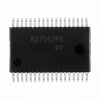
M37542F8FP#U0 Renesas Electronics America, M37542F8FP#U0 Datasheet - Page 112

M37542F8FP#U0
Manufacturer Part Number
M37542F8FP#U0
Description
IC 740 MCU FLASH 32K 36SSOP
Manufacturer
Renesas Electronics America
Series
740/38000r
Datasheet
1.M37542F8FPU0.pdf
(124 pages)
Specifications of M37542F8FP#U0
Core Processor
740
Core Size
8-Bit
Speed
8MHz
Connectivity
SIO, UART/USART
Peripherals
WDT
Number Of I /o
29
Program Memory Size
32KB (32K x 8)
Program Memory Type
FLASH
Ram Size
1K x 8
Voltage - Supply (vcc/vdd)
2.2 V ~ 5.5 V
Data Converters
A/D 8x10b
Oscillator Type
Internal
Operating Temperature
-20°C ~ 85°C
Package / Case
36-SSOP
Lead Free Status / RoHS Status
Lead free / RoHS Compliant
Eeprom Size
-
Available stocks
Company
Part Number
Manufacturer
Quantity
Price
7542 Group
6. Direction register
The values of the port direction registers cannot be read.
That is, it is impossible to use the LDA instruction, memory opera-
tion instruction when the T flag is “1”, addressing mode using
direction register values as qualifiers, and bit test instructions such
as BBC and BBS.
It is also impossible to use bit operation instructions such as CLB
and SEB and read-modify-write instructions of direction registers
for calculations such as ROR.
For setting direction registers, use the LDM instruction, STA in-
struction, etc.
Termination of Unused Pins
1. Terminate unused pins
Perform the following wiring at the shortest possible distance (20
mm or less) from microcomputer pins.
(1) I/O ports
Set the I/O ports for the input mode and connect each pin to V
or V
select a built-in pull-up resistor can also use the built-in pull-up re-
sistor.
When using the I/O ports as the output mode, open them at “L” or
“H”.
• When opening them in the output mode, the input mode of the
• Since the direction register setup may be changed because of a
2. Termination remarks
(1) I/O ports setting as input mode
[1] Do not open in the input mode.
<Reason>
[2] Do not connect to V
<Reason>
If the direction register setup changes for the output mode be-
cause of a program runaway or noise, a short circuit may occur.
[3] Do not connect multiple ports in a lump to V
<Reason>
If the direction register setup changes for the output mode be-
cause of a program runaway or noise, a short circuit may occur
between ports.
Rev.3.03
REJ03B0006-0303
• The power source current may increase depending on the first-
• An effect due to noise may be easily produced as compared with
initial status remains until the mode of the ports is switched over
to the output mode by the program after reset. Thus, the poten-
tial at these pins is undefined and the power source current may
increase in the input mode. With regard to an effects on the sys-
tem, thoroughly perform system evaluation on the user side.
program runaway or noise, set direction registers by program
periodically to increase the reliability of program.
stage circuit.
proper termination (1) shown on the above “1. Terminate unused
pins”.
a resistor.
SS
through each resistor of 1 kΩ to 10 kΩ. The port which can
Jul 11, 2008
CC
or V
SS
Page 110 of 117
directly.
CC
or V
SS
through
CC
Fig. 4 Sequence of changing relevant register
<Reason>
When setting the followings, the interrupt request bit of the corre-
sponding interrupt may be set to “1”.
• When switching external interrupt active edge
2. Check of interrupt request bit
When executing the BBC or BBS instruction to determine an in-
terrupt request bit immediately after this bit is set to “0”, take the
following sequence.
<Reason>
If the BBC or BBS instruction is executed immediately after an in-
terrupt request bit is cleared to “0”, the value of the interrupt
request bit before being cleared to “0” is read.
Fig. 5 Sequence of check of interrupt request bit
Notes on Interrupts
1. Change of relevant register settings
When not requiring for the interrupt occurrence synchronous with
the following case, take the sequence shown in Figure 4.
• When switching external interrupt active edge
• When switching interrupt sources of an interrupt vector address
INT
(bit 0 of Interrupt edge selection register (address 3A
INT
(bit 1 of Interrupt edge selection register)
CNTR
(bit 2 of timer X mode register (address 2B
Capture 0 interrupt edge selection bit
(bits 1 and 0 of capture mode register (address 20
Capture 1 interrupt edge selection bit
(bits 3 and 2 of capture mode register)
where two or more interrupt sources are allocated
Set the interrupt edge selection bit, active edge switch bit, or
Set the corresponding interrupt enable bit to “0” (disabled) .
Set the corresponding interrupt enable bit to “1” (enabled).
0
1
Set the interrupt request bit to “0” (no interrupt issued)
interrupt edge selection bit
interrupt edge selection bit
0
Set the corresponding interrupt request bit to “0”
active edge switch bit
Execute the BBC or BBS instruction
the interrupt source selection bit.
NOP (One or more instructions)
NOP (one or more instructions)
(no interrupt request issued).
↓
↓
↓
↓
↓
↓
16
))
16
))
16
))


