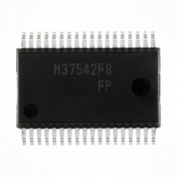
M37542F8FP#U0 Renesas Electronics America, M37542F8FP#U0 Datasheet - Page 79

M37542F8FP#U0
Manufacturer Part Number
M37542F8FP#U0
Description
IC 740 MCU FLASH 32K 36SSOP
Manufacturer
Renesas Electronics America
Series
740/38000r
Datasheet
1.M37542F8FPU0.pdf
(124 pages)
Specifications of M37542F8FP#U0
Core Processor
740
Core Size
8-Bit
Speed
8MHz
Connectivity
SIO, UART/USART
Peripherals
WDT
Number Of I /o
29
Program Memory Size
32KB (32K x 8)
Program Memory Type
FLASH
Ram Size
1K x 8
Voltage - Supply (vcc/vdd)
2.2 V ~ 5.5 V
Data Converters
A/D 8x10b
Oscillator Type
Internal
Operating Temperature
-20°C ~ 85°C
Package / Case
36-SSOP
Lead Free Status / RoHS Status
Lead free / RoHS Compliant
Eeprom Size
-
Available stocks
Company
Part Number
Manufacturer
Quantity
Price
7542 Group
Figure 101 shows a flowchart for setting/releasing CPU rewrite mode.
Fig. 101 CPU rewrite mode set/release flowchart
Take the notes described below when rewriting the flash memory
in CPU rewrite mode.
During CPU rewrite mode, set the system clock φ to 4.0 MHz or
less using the clock division ratio selection bits (bits 6 and 7 of ad-
dress 003B
The instructions which refer to the internal data of the flash
memory cannot be used during CPU rewrite mode.
Rev.3.03
REJ03B0006-0303
Operation speed
Instructions inhibited against use
Notes on CPU Rewrite Mode
16
).
Jul 11, 2008
N o t e s 1: S e t t h e m a i n c l o c k a s f o l l o w s d e p e n d i n g o n t h e c l o c k d i v i s i o n r a t i o s e l e c t i o n b i t s o f
Page 77 of 117
2: As for setting of these bits, refer to Table 10.
3: Before exiting the CPU rewrite mode after completing erase or program operation,
CPU mode register (bits 6, 7 of address 003B
a l w a y s b e s u r e t o e x e c u t e t h e r e a d a r r a y c o m m a n d o r r e s e t t h e f l a s h m e m o r y .
J u m p t o c o n t r o l p r o g r a m t r a n s f e r r e d t o i n t e r n a l R A M
( S u b s e q u e n t o p e r a t i o n s a r e e x e c u t e d b y c o n t r o l
p r o g r a m i n t h i s R A M )
S e t a l l u s e r b l o c k E / W e n a b l e b i t t o “ 0 ”
S e t 8 K B u s e r b l o c k E / W m o d e e n a b l e b i t t o “ 0 ”
S e t a l l u s e r b l o c k E / W e n a b l e b i t
S e t 8 K B u s e r b l o c k E / W m o d e e n a b l e b i t
(f o r s e t t i n g t o “ 1 ”, b y w r i t i n g “ 0 ” a n d t h e n “ 1 ”
i n s u c c e s s i o n )
(Note 2)
Single-chip mode or Boot mode
Execute read array command or reset flash
memory by setting flash memory reset bit (by
writing “1” and then “0” in succession) (Note 3)
Set CPU mode register (Note 1)
T r a n s f e r C P U r e w r i t e m o d e c o n t r o l p r o g r a m t o
i n t e r n a l R A M
Using software command executes erase,
program, or other operation
Write “0” to CPU rewrite mode select bit
S e t C P U r e w r i t e m o d e s e l e c t b i t t o “ 1 ”
( b y w r i t i n g “ 0 ” a n d t h e n “ 1 ” i n s u c c e s s i o n )
Start
End
16
The interrupts cannot be used during CPU rewrite mode because
they refer to the internal data of the flash memory.
If the watchdog timer has been already activated, internal reset
due to an underflow will not occur because the watchdog timer is
surely cleared during program or erase.
Reset is always valid. The MCU is activated using the boot mode
at release of reset in the condition of CNVss = “H”, so that the pro-
gram will begin at the address which is stored in addresses
FFFC
).
Interrupts inhibited against use
Watchdog timer
Reset
16
and FFFD
16
of the boot ROM area.


