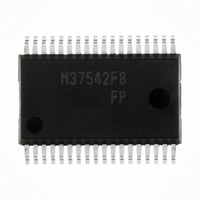
M37542F8FP#U0 Renesas Electronics America, M37542F8FP#U0 Datasheet - Page 81

M37542F8FP#U0
Manufacturer Part Number
M37542F8FP#U0
Description
IC 740 MCU FLASH 32K 36SSOP
Manufacturer
Renesas Electronics America
Series
740/38000r
Datasheet
1.M37542F8FPU0.pdf
(124 pages)
Specifications of M37542F8FP#U0
Core Processor
740
Core Size
8-Bit
Speed
8MHz
Connectivity
SIO, UART/USART
Peripherals
WDT
Number Of I /o
29
Program Memory Size
32KB (32K x 8)
Program Memory Type
FLASH
Ram Size
1K x 8
Voltage - Supply (vcc/vdd)
2.2 V ~ 5.5 V
Data Converters
A/D 8x10b
Oscillator Type
Internal
Operating Temperature
-20°C ~ 85°C
Package / Case
36-SSOP
Lead Free Status / RoHS Status
Lead free / RoHS Compliant
Eeprom Size
-
Available stocks
Company
Part Number
Manufacturer
Quantity
Price
7542 Group
• Block Erase Command (20
By writing the command code “20
confirmation command code “D0
second bus cycle that follows, the block erase (erase and erase
verify) operation starts for the block address of the flash memory
to be specified.
Whether the block erase operation is completed can be confirmed
by read status register or the RY/BY status flag of flash memory
control register. At the same time the block erase operation starts,
the read status register mode is automatically entered, so that the
contents of the status register can be read out. The status register
bit 7 (SR7) is set to “0” at the same time the block erase operation
starts and is returned to “1” upon completion of the block erase
operation. In this case, the read status register mode remains ac-
tive until the read array command (FF
The RY/BY status flag is “0” during block erase operation and “1”
when the block erase operation is completed as is the status reg-
ister bit 7.
After the block erase ends, erase results can be checked by read-
ing the status register. For details, refer to the section where the
status register is detailed.
Rev.3.03
REJ03B0006-0303
Jul 11, 2008
16
/D0
Page 79 of 117
16
16
” and the block address in the
16
” in the first bus cycle and the
)
16
) is written.
Fig. 103 Erase flowchart
Write
(write read command “
Read status register
Erase completed
SR5 = “0” ?
RY/BY = “1”?
Write “20
SR7 = “1”?
Block address
FF
Start
16
or
“D0
YES
”
YES
)
16
16
”
”
NO
NO
Erase error


