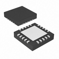
PIC16F689-I/ML Microchip Technology, PIC16F689-I/ML Datasheet - Page 109

PIC16F689-I/ML
Manufacturer Part Number
PIC16F689-I/ML
Description
IC PIC MCU FLASH 4KX14 20QFN
Manufacturer
Microchip Technology
Series
PIC® 16Fr
Datasheets
1.PIC16F616T-ISL.pdf
(8 pages)
2.PIC16F690DM-PCTLHS.pdf
(306 pages)
3.PIC16F677-IP.pdf
(2 pages)
4.PIC16F677-IP.pdf
(16 pages)
5.PIC16F689-IML.pdf
(294 pages)
Specifications of PIC16F689-I/ML
Program Memory Type
FLASH
Program Memory Size
7KB (4K x 14)
Package / Case
20-VQFN Exposed Pad, 20-HVQFN, 20-SQFN, 20-DHVQFN
Core Processor
PIC
Core Size
8-Bit
Speed
20MHz
Connectivity
I²C, SPI, UART/USART
Peripherals
Brown-out Detect/Reset, POR, WDT
Number Of I /o
18
Eeprom Size
256 x 8
Ram Size
256 x 8
Voltage - Supply (vcc/vdd)
2 V ~ 5.5 V
Data Converters
A/D 12x10b
Oscillator Type
Internal
Operating Temperature
-40°C ~ 85°C
Processor Series
PIC16F
Core
PIC
Data Bus Width
8 bit
Data Ram Size
256 B
Interface Type
I2C/SPI/SSP/EUSART
Maximum Clock Frequency
20 MHz
Number Of Programmable I/os
17
Number Of Timers
2
Maximum Operating Temperature
+ 85 C
Mounting Style
SMD/SMT
3rd Party Development Tools
52715-96, 52716-328, 52717-734
Development Tools By Supplier
PG164130, DV164035, DV244005, DV164005, PG164120, ICE2000, DM163029, DM164120
Minimum Operating Temperature
- 40 C
On-chip Adc
12-ch x 10-bit
Lead Free Status / RoHS Status
Lead free / RoHS Compliant
For Use With
AC164324 - MODULE SKT FOR MPLAB 8DFN/16QFNAC162061 - HEADER INTRFC MPLAB ICD2 20PIN
Lead Free Status / Rohs Status
Lead free / RoHS Compliant
- PIC16F616T-ISL PDF datasheet
- PIC16F690DM-PCTLHS PDF datasheet #2
- PIC16F677-IP PDF datasheet #3
- PIC16F677-IP PDF datasheet #4
- PIC16F689-IML PDF datasheet #5
- Current page: 109 of 294
- Download datasheet (6Mb)
9.0
The
conversion of an analog input signal to a 10-bit binary
representation of that signal. This device uses analog
inputs, which are multiplexed into a single sample and
hold circuit. The output of the sample and hold is
connected to the input of the converter. The converter
generates a 10-bit binary result via successive
approximation and stores the conversion result into the
ADC result registers (ADRESL and ADRESH).
The ADC voltage reference is software selectable to
either V
pins.
The ADC can generate an interrupt upon completion of
a conversion. This interrupt can be used to wake-up the
device from Sleep.
FIGURE 9-1:
© 2007 Microchip Technology Inc.
Note:
Analog-to-Digital
DD
ANALOG-TO-DIGITAL
CONVERTER (ADC) MODULE
RA0/AN0/C1IN+/ICSPDAT/ULPWU
Note 1:
RA1/AN1/C12IN0-/V
or a voltage applied to the external reference
The ADC module applies to PIC16F677/
PIC16F685/PIC16F687/PIC16F689/
PIC16F690 devices only.
RA4/AN3/T1G/OSC2/CLKOUT
RA2/AN2/T0CKI/INT/C1OUT
2:
3:
RC2/AN6/C12IN2-/P1D
RC3/AN7/C12IN3-/P1C
RB4/AN10/SDI/SDA
P1C and P1D available on PIC16F685/PIC16F690 only.
SS, SDO, SDA, RX and DT available on PIC16F677/PIC16F687/PIC16F689/PIC16F690 only.
ADC module applies to the PIC16F677/PIC16F685/PIC16F687/PIC16F689/PIC16F690 devices only.
ADC BLOCK DIAGRAM
RB5/AN11/RX/DT
RC1/AN5/C12IN1-
RC7/AN9/SDO
Converter
RC0/AN4/C2IN+
RC6/AN8/SS
VP6 Reference
REF
/ICSPCLK
CV
PIC16F631/677/685/687/689/690
REF
(ADC)
(1)
(1)
(2)
(2)
(2)
(2)
CHS
allows
V
REF
V
DD
GO/DONE
Figure 9-1 shows the block diagram of the ADC.
VCFG = 0
VCFG = 1
ADON
V
SS
ADC
ADFM
ADRESH ADRESL
0 = Left Justify
1 = Right Justify
DS41262D-page 107
10
10
Related parts for PIC16F689-I/ML
Image
Part Number
Description
Manufacturer
Datasheet
Request
R

Part Number:
Description:
IC PIC MCU FLASH 4KX14 20SSOP
Manufacturer:
Microchip Technology
Datasheet:

Part Number:
Description:
IC PIC MCU FLASH 4KX14 20SOIC
Manufacturer:
Microchip Technology
Datasheet:

Part Number:
Description:
IC PIC MCU FLASH 4KX14 20DIP
Manufacturer:
Microchip Technology
Datasheet:

Part Number:
Description:
IC PIC MCU FLASH 4KX14 20DIP
Manufacturer:
Microchip Technology
Datasheet:

Part Number:
Description:
IC,MICROCONTROLLER,8-BIT,PIC CPU,CMOS,LLCC,20PIN,PLASTIC
Manufacturer:
Microchip Technology
Datasheet:

Part Number:
Description:
IC,MICROCONTROLLER,8-BIT,PIC CPU,CMOS,SOP,20PIN,PLASTIC
Manufacturer:
Microchip Technology
Datasheet:

Part Number:
Description:
IC,MICROCONTROLLER,8-BIT,PIC CPU,CMOS,SSOP,20PIN,PLASTIC
Manufacturer:
Microchip Technology
Datasheet:

Part Number:
Description:
(PIC16F6xx) 20-Pin Flash Based / 8-Bit CMOS Microcontrollers
Manufacturer:
Microchip Technology

Part Number:
Description:
IC, 8BIT MCU, PIC16F, 32MHZ, SOIC-18
Manufacturer:
Microchip Technology
Datasheet:

Part Number:
Description:
IC, 8BIT MCU, PIC16F, 32MHZ, SSOP-20
Manufacturer:
Microchip Technology
Datasheet:

Part Number:
Description:
IC, 8BIT MCU, PIC16F, 32MHZ, DIP-18
Manufacturer:
Microchip Technology
Datasheet:

Part Number:
Description:
IC, 8BIT MCU, PIC16F, 32MHZ, QFN-28
Manufacturer:
Microchip Technology
Datasheet:

Part Number:
Description:
IC, 8BIT MCU, PIC16F, 32MHZ, QFN-28
Manufacturer:
Microchip Technology
Datasheet:

Part Number:
Description:
IC, 8BIT MCU, PIC16F, 32MHZ, QFN-28
Manufacturer:
Microchip Technology
Datasheet:

Part Number:
Description:
IC, 8BIT MCU, PIC16F, 32MHZ, SSOP-20
Manufacturer:
Microchip Technology
Datasheet:


