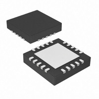
PIC16F689-I/ML Microchip Technology, PIC16F689-I/ML Datasheet - Page 256

PIC16F689-I/ML
Manufacturer Part Number
PIC16F689-I/ML
Description
IC PIC MCU FLASH 4KX14 20QFN
Manufacturer
Microchip Technology
Series
PIC® 16Fr
Datasheets
1.PIC16F616T-ISL.pdf
(8 pages)
2.PIC16F690DM-PCTLHS.pdf
(306 pages)
3.PIC16F677-IP.pdf
(2 pages)
4.PIC16F677-IP.pdf
(16 pages)
5.PIC16F689-IML.pdf
(294 pages)
Specifications of PIC16F689-I/ML
Program Memory Type
FLASH
Program Memory Size
7KB (4K x 14)
Package / Case
20-VQFN Exposed Pad, 20-HVQFN, 20-SQFN, 20-DHVQFN
Core Processor
PIC
Core Size
8-Bit
Speed
20MHz
Connectivity
I²C, SPI, UART/USART
Peripherals
Brown-out Detect/Reset, POR, WDT
Number Of I /o
18
Eeprom Size
256 x 8
Ram Size
256 x 8
Voltage - Supply (vcc/vdd)
2 V ~ 5.5 V
Data Converters
A/D 12x10b
Oscillator Type
Internal
Operating Temperature
-40°C ~ 85°C
Processor Series
PIC16F
Core
PIC
Data Bus Width
8 bit
Data Ram Size
256 B
Interface Type
I2C/SPI/SSP/EUSART
Maximum Clock Frequency
20 MHz
Number Of Programmable I/os
17
Number Of Timers
2
Maximum Operating Temperature
+ 85 C
Mounting Style
SMD/SMT
3rd Party Development Tools
52715-96, 52716-328, 52717-734
Development Tools By Supplier
PG164130, DV164035, DV244005, DV164005, PG164120, ICE2000, DM163029, DM164120
Minimum Operating Temperature
- 40 C
On-chip Adc
12-ch x 10-bit
Lead Free Status / RoHS Status
Lead free / RoHS Compliant
For Use With
AC164324 - MODULE SKT FOR MPLAB 8DFN/16QFNAC162061 - HEADER INTRFC MPLAB ICD2 20PIN
Lead Free Status / Rohs Status
Lead free / RoHS Compliant
- PIC16F616T-ISL PDF datasheet
- PIC16F690DM-PCTLHS PDF datasheet #2
- PIC16F677-IP PDF datasheet #3
- PIC16F677-IP PDF datasheet #4
- PIC16F689-IML PDF datasheet #5
- Current page: 256 of 294
- Download datasheet (6Mb)
PIC16F631/677/685/687/689/690
FIGURE 17-19:
TABLE 17-17: A/D CONVERSION REQUIREMENTS (SLEEP MODE)
DS41262D-page 254
Standard Operating Conditions (unless otherwise stated)
Operating Temperature
130
131
132
134
Note 1:
Param
No.
Note 1: If the A/D clock source is selected as RC, a time of T
A/D Data
A/D CLK
2:
BSF ADCON0, GO
ADRES
Sample
*
† Data in “Typ” column is at 5.0V, 25°C unless otherwise stated. These parameters are for design guidance
ADIF
GO
These parameters are characterized but not tested.
only and are not tested.
ADRES register may be read on the following T
See Table 9-1 for minimum conditions.
T
T
T
T
Q4
CNV
ACQ
Sym
AD
GO
SLEEP instruction to be executed.
134
132
A/D Internal RC
Oscillator Period
Conversion Time
(not including
Acquisition Time)
Acquisition Time
Q4 to A/D Clock
Start
Characteristic
A/D CONVERSION TIMING (SLEEP MODE)
-40°C ≤ T
(T
OSC
/2 + T
A
(1)
≤ +125°C
CY
9
)
(1)
Min
3.0*
2.0*
—
(2)
5*
—
OLD_DATA
Sampling Stopped
8
T
OSC
Typ†
7
11.5
6.0
4.0
/2 + T
131
11
—
CY
cycle.
6
CY
CY
130
is added before the A/D clock starts. This allows the
Max
9.0*
6.0*
—
—
—
—
3
Units
2
T
μs
μs
μs
μs
—
AD
ADCS<1:0> = 11 (RC mode)
At V
At V
The minimum time is the amplifier
settling time. This may be used if
the “new” input voltage has not
changed by more than 1 LSb (i.e.,
4.1 mV @ 4.096V) from the last
sampled voltage (as stored on
C
If the A/D clock source is selected
as RC, a time of T
before the A/D clock starts. This
allows the SLEEP instruction to be
executed.
1
HOLD
© 2007 Microchip Technology Inc.
DD
DD
).
0
= 2.5V
= 5.0V
NEW_DATA
Conditions
1 T
DONE
CY
1 T
CY
CY
is added
Related parts for PIC16F689-I/ML
Image
Part Number
Description
Manufacturer
Datasheet
Request
R

Part Number:
Description:
IC PIC MCU FLASH 4KX14 20SSOP
Manufacturer:
Microchip Technology
Datasheet:

Part Number:
Description:
IC PIC MCU FLASH 4KX14 20SOIC
Manufacturer:
Microchip Technology
Datasheet:

Part Number:
Description:
IC PIC MCU FLASH 4KX14 20DIP
Manufacturer:
Microchip Technology
Datasheet:

Part Number:
Description:
IC PIC MCU FLASH 4KX14 20DIP
Manufacturer:
Microchip Technology
Datasheet:

Part Number:
Description:
IC,MICROCONTROLLER,8-BIT,PIC CPU,CMOS,LLCC,20PIN,PLASTIC
Manufacturer:
Microchip Technology
Datasheet:

Part Number:
Description:
IC,MICROCONTROLLER,8-BIT,PIC CPU,CMOS,SOP,20PIN,PLASTIC
Manufacturer:
Microchip Technology
Datasheet:

Part Number:
Description:
IC,MICROCONTROLLER,8-BIT,PIC CPU,CMOS,SSOP,20PIN,PLASTIC
Manufacturer:
Microchip Technology
Datasheet:

Part Number:
Description:
(PIC16F6xx) 20-Pin Flash Based / 8-Bit CMOS Microcontrollers
Manufacturer:
Microchip Technology

Part Number:
Description:
IC, 8BIT MCU, PIC16F, 32MHZ, SOIC-18
Manufacturer:
Microchip Technology
Datasheet:

Part Number:
Description:
IC, 8BIT MCU, PIC16F, 32MHZ, SSOP-20
Manufacturer:
Microchip Technology
Datasheet:

Part Number:
Description:
IC, 8BIT MCU, PIC16F, 32MHZ, DIP-18
Manufacturer:
Microchip Technology
Datasheet:

Part Number:
Description:
IC, 8BIT MCU, PIC16F, 32MHZ, QFN-28
Manufacturer:
Microchip Technology
Datasheet:

Part Number:
Description:
IC, 8BIT MCU, PIC16F, 32MHZ, QFN-28
Manufacturer:
Microchip Technology
Datasheet:

Part Number:
Description:
IC, 8BIT MCU, PIC16F, 32MHZ, QFN-28
Manufacturer:
Microchip Technology
Datasheet:

Part Number:
Description:
IC, 8BIT MCU, PIC16F, 32MHZ, SSOP-20
Manufacturer:
Microchip Technology
Datasheet:


