PIC16F689-I/ML Microchip Technology, PIC16F689-I/ML Datasheet - Page 66
PIC16F689-I/ML
Manufacturer Part Number
PIC16F689-I/ML
Description
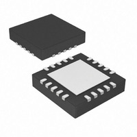
IC PIC MCU FLASH 4KX14 20QFN
Manufacturer
Microchip Technology
Series
PIC® 16Fr
Datasheets
1.PIC16F616T-ISL.pdf
(8 pages)
2.PIC16F690DM-PCTLHS.pdf
(306 pages)
3.PIC16F677-IP.pdf
(2 pages)
4.PIC16F677-IP.pdf
(16 pages)
5.PIC16F689-IML.pdf
(294 pages)
Specifications of PIC16F689-I/ML
Program Memory Type
FLASH
Program Memory Size
7KB (4K x 14)
Package / Case
20-VQFN Exposed Pad, 20-HVQFN, 20-SQFN, 20-DHVQFN
Core Processor
PIC
Core Size
8-Bit
Speed
20MHz
Connectivity
I²C, SPI, UART/USART
Peripherals
Brown-out Detect/Reset, POR, WDT
Number Of I /o
18
Eeprom Size
256 x 8
Ram Size
256 x 8
Voltage - Supply (vcc/vdd)
2 V ~ 5.5 V
Data Converters
A/D 12x10b
Oscillator Type
Internal
Operating Temperature
-40°C ~ 85°C
Processor Series
PIC16F
Core
PIC
Data Bus Width
8 bit
Data Ram Size
256 B
Interface Type
I2C/SPI/SSP/EUSART
Maximum Clock Frequency
20 MHz
Number Of Programmable I/os
17
Number Of Timers
2
Maximum Operating Temperature
+ 85 C
Mounting Style
SMD/SMT
3rd Party Development Tools
52715-96, 52716-328, 52717-734
Development Tools By Supplier
PG164130, DV164035, DV244005, DV164005, PG164120, ICE2000, DM163029, DM164120
Minimum Operating Temperature
- 40 C
On-chip Adc
12-ch x 10-bit
Lead Free Status / RoHS Status
Lead free / RoHS Compliant
For Use With
AC164324 - MODULE SKT FOR MPLAB 8DFN/16QFNAC162061 - HEADER INTRFC MPLAB ICD2 20PIN
Lead Free Status / Rohs Status
Lead free / RoHS Compliant


PIC16F631/677/685/687/689/690
4.2.5
Each PORTA pin is multiplexed with other functions. The
pins and their combined functions are briefly described
here. For specific information about individual functions
such as the comparator or the A/D Converter (ADC),
refer to the appropriate section in this data sheet.
FIGURE 4-1:
DS41262D-page 64
PIN DESCRIPTIONS AND
DIAGRAMS
Interrupt-on-Change
Data Bus
WPUDA
WPUDA
PORTA
PORTA
Note 1:
TRISA
TRISA
IOCA
IOCA
WR
RD
WR
WR
WR
RD
RD
RD
BLOCK DIAGRAM OF RA0
2:
D
D
D
D
ANSEL determines Analog Input mode.
Not implemented on PIC16F631.
CK
CK
CK
CK
Q
Q
Q
Q
Q
Q
Q
Q
To A/D Converter
To Comparator
RD PORTA
Input Mode
Analog
(2)
Q
Q
(1)
Input Mode
Analog
EN
EN
4.2.5.1
Figure 4-2 shows the diagram for this pin. The
RA0/AN0/C1IN+/ICSPDAT/ULPWU pin is configurable
to function as one of the following:
• a general purpose I/O
• an analog input for the ADC (except PIC16F631)
• an analog input to Comparator C1
• In-Circuit Serial Programming™ data
• an analog input for the Ultra Low-Power Wake-up
D
D
0
(1)
RABPU
1
Q3
+
-
RA0/AN0/C1IN+/ICSPDAT/ULPWU
ULPWUE
V
Weak
DD
I
ULP
V
SS
© 2007 Microchip Technology Inc.
V
T
V
V
DD
SS
I/O Pin
Related parts for PIC16F689-I/ML
Image
Part Number
Description
Manufacturer
Datasheet
Request
R

Part Number:
Description:
IC PIC MCU FLASH 4KX14 20SSOP
Manufacturer:
Microchip Technology
Datasheet:

Part Number:
Description:
IC PIC MCU FLASH 4KX14 20SOIC
Manufacturer:
Microchip Technology
Datasheet:

Part Number:
Description:
IC PIC MCU FLASH 4KX14 20DIP
Manufacturer:
Microchip Technology
Datasheet:
Part Number:
Description:
IC PIC MCU FLASH 4KX14 20DIP
Manufacturer:
Microchip Technology
Datasheet:

Part Number:
Description:
IC,MICROCONTROLLER,8-BIT,PIC CPU,CMOS,LLCC,20PIN,PLASTIC
Manufacturer:
Microchip Technology
Datasheet:

Part Number:
Description:
IC,MICROCONTROLLER,8-BIT,PIC CPU,CMOS,SOP,20PIN,PLASTIC
Manufacturer:
Microchip Technology
Datasheet:
Part Number:
Description:
IC,MICROCONTROLLER,8-BIT,PIC CPU,CMOS,SSOP,20PIN,PLASTIC
Manufacturer:
Microchip Technology
Datasheet:
Part Number:
Description:
(PIC16F6xx) 20-Pin Flash Based / 8-Bit CMOS Microcontrollers
Manufacturer:
Microchip Technology

Part Number:
Description:
IC, 8BIT MCU, PIC16F, 32MHZ, SOIC-18
Manufacturer:
Microchip Technology
Datasheet:

Part Number:
Description:
IC, 8BIT MCU, PIC16F, 32MHZ, SSOP-20
Manufacturer:
Microchip Technology
Datasheet:
Part Number:
Description:
IC, 8BIT MCU, PIC16F, 32MHZ, DIP-18
Manufacturer:
Microchip Technology
Datasheet:

Part Number:
Description:
IC, 8BIT MCU, PIC16F, 32MHZ, QFN-28
Manufacturer:
Microchip Technology
Datasheet:

Part Number:
Description:
IC, 8BIT MCU, PIC16F, 32MHZ, QFN-28
Manufacturer:
Microchip Technology
Datasheet:
Part Number:
Description:
IC, 8BIT MCU, PIC16F, 32MHZ, QFN-28
Manufacturer:
Microchip Technology
Datasheet:
Part Number:
Description:
IC, 8BIT MCU, PIC16F, 32MHZ, SSOP-20
Manufacturer:
Microchip Technology
Datasheet: