PIC16F689-I/ML Microchip Technology, PIC16F689-I/ML Datasheet - Page 142
PIC16F689-I/ML
Manufacturer Part Number
PIC16F689-I/ML
Description
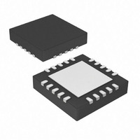
IC PIC MCU FLASH 4KX14 20QFN
Manufacturer
Microchip Technology
Series
PIC® 16Fr
Datasheets
1.PIC16F616T-ISL.pdf
(8 pages)
2.PIC16F690DM-PCTLHS.pdf
(306 pages)
3.PIC16F677-IP.pdf
(2 pages)
4.PIC16F677-IP.pdf
(16 pages)
5.PIC16F689-IML.pdf
(294 pages)
Specifications of PIC16F689-I/ML
Program Memory Type
FLASH
Program Memory Size
7KB (4K x 14)
Package / Case
20-VQFN Exposed Pad, 20-HVQFN, 20-SQFN, 20-DHVQFN
Core Processor
PIC
Core Size
8-Bit
Speed
20MHz
Connectivity
I²C, SPI, UART/USART
Peripherals
Brown-out Detect/Reset, POR, WDT
Number Of I /o
18
Eeprom Size
256 x 8
Ram Size
256 x 8
Voltage - Supply (vcc/vdd)
2 V ~ 5.5 V
Data Converters
A/D 12x10b
Oscillator Type
Internal
Operating Temperature
-40°C ~ 85°C
Processor Series
PIC16F
Core
PIC
Data Bus Width
8 bit
Data Ram Size
256 B
Interface Type
I2C/SPI/SSP/EUSART
Maximum Clock Frequency
20 MHz
Number Of Programmable I/os
17
Number Of Timers
2
Maximum Operating Temperature
+ 85 C
Mounting Style
SMD/SMT
3rd Party Development Tools
52715-96, 52716-328, 52717-734
Development Tools By Supplier
PG164130, DV164035, DV244005, DV164005, PG164120, ICE2000, DM163029, DM164120
Minimum Operating Temperature
- 40 C
On-chip Adc
12-ch x 10-bit
Lead Free Status / RoHS Status
Lead free / RoHS Compliant
For Use With
AC164324 - MODULE SKT FOR MPLAB 8DFN/16QFNAC162061 - HEADER INTRFC MPLAB ICD2 20PIN
Lead Free Status / Rohs Status
Lead free / RoHS Compliant


PIC16F631/677/685/687/689/690
FIGURE 11-13:
11.4.3
When any PWM mode is used, the application
hardware must use the proper external pull-up and/or
pull-down resistors on the PWM output pins.
The CCP1M<1:0> bits of the CCP1CON register allow
the user to choose whether the PWM output signals are
active-high or active-low for each pair of PWM output pins
(P1A/P1C and P1B/P1D). The PWM output polarities
must be selected before the PWM pin output drivers are
enabled. Changing the polarity configuration while the
PWM pin output drivers are enabled is not recommended
since it may result in damage to the application circuits.
The P1A, P1B, P1C and P1D output latches may not be
in the proper states when the PWM module is
initialized. Enabling the PWM pin output drivers at the
same time as the Enhanced PWM modes may cause
damage to the application circuit. The Enhanced PWM
modes must be enabled in the proper Output mode and
complete a full PWM cycle before enabling the PWM
pin output drivers. The completion of a full PWM cycle
is indicated by the TMR2IF bit of the PIR1 register
being set as the second PWM period begins.
DS41262D-page 140
Note:
Shoot-Through Current
Note 1: All signals are shown as active-high.
External Switch C
External Switch D
START-UP CONSIDERATIONS
When the microcontroller is released from
Reset, all of the I/O pins are in the
high-impedance state. The external cir-
cuits must keep the power switch devices
in the OFF state until the microcontroller
drives the I/O pins with the proper signal
levels or activates the PWM output(s).
2: T
3: T
ON
OFF
Potential
is the turn on delay of power switch QC and its driver.
is the turn off delay of power switch QD and its driver.
P1C
P1D
P1A
P1B
EXAMPLE OF PWM DIRECTION CHANGE AT NEAR 100% DUTY CYCLE
Forward Period
PW
t1
T
ON
Reverse Period
T
T = T
OFF
OFF
PW
© 2007 Microchip Technology Inc.
– T
ON
Related parts for PIC16F689-I/ML
Image
Part Number
Description
Manufacturer
Datasheet
Request
R

Part Number:
Description:
IC PIC MCU FLASH 4KX14 20SSOP
Manufacturer:
Microchip Technology
Datasheet:

Part Number:
Description:
IC PIC MCU FLASH 4KX14 20SOIC
Manufacturer:
Microchip Technology
Datasheet:

Part Number:
Description:
IC PIC MCU FLASH 4KX14 20DIP
Manufacturer:
Microchip Technology
Datasheet:
Part Number:
Description:
IC PIC MCU FLASH 4KX14 20DIP
Manufacturer:
Microchip Technology
Datasheet:

Part Number:
Description:
IC,MICROCONTROLLER,8-BIT,PIC CPU,CMOS,LLCC,20PIN,PLASTIC
Manufacturer:
Microchip Technology
Datasheet:

Part Number:
Description:
IC,MICROCONTROLLER,8-BIT,PIC CPU,CMOS,SOP,20PIN,PLASTIC
Manufacturer:
Microchip Technology
Datasheet:
Part Number:
Description:
IC,MICROCONTROLLER,8-BIT,PIC CPU,CMOS,SSOP,20PIN,PLASTIC
Manufacturer:
Microchip Technology
Datasheet:
Part Number:
Description:
(PIC16F6xx) 20-Pin Flash Based / 8-Bit CMOS Microcontrollers
Manufacturer:
Microchip Technology

Part Number:
Description:
IC, 8BIT MCU, PIC16F, 32MHZ, SOIC-18
Manufacturer:
Microchip Technology
Datasheet:

Part Number:
Description:
IC, 8BIT MCU, PIC16F, 32MHZ, SSOP-20
Manufacturer:
Microchip Technology
Datasheet:
Part Number:
Description:
IC, 8BIT MCU, PIC16F, 32MHZ, DIP-18
Manufacturer:
Microchip Technology
Datasheet:

Part Number:
Description:
IC, 8BIT MCU, PIC16F, 32MHZ, QFN-28
Manufacturer:
Microchip Technology
Datasheet:

Part Number:
Description:
IC, 8BIT MCU, PIC16F, 32MHZ, QFN-28
Manufacturer:
Microchip Technology
Datasheet:
Part Number:
Description:
IC, 8BIT MCU, PIC16F, 32MHZ, QFN-28
Manufacturer:
Microchip Technology
Datasheet:
Part Number:
Description:
IC, 8BIT MCU, PIC16F, 32MHZ, SSOP-20
Manufacturer:
Microchip Technology
Datasheet: