PIC16F689-I/ML Microchip Technology, PIC16F689-I/ML Datasheet - Page 185
PIC16F689-I/ML
Manufacturer Part Number
PIC16F689-I/ML
Description
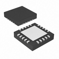
IC PIC MCU FLASH 4KX14 20QFN
Manufacturer
Microchip Technology
Series
PIC® 16Fr
Datasheets
1.PIC16F616T-ISL.pdf
(8 pages)
2.PIC16F690DM-PCTLHS.pdf
(306 pages)
3.PIC16F677-IP.pdf
(2 pages)
4.PIC16F677-IP.pdf
(16 pages)
5.PIC16F689-IML.pdf
(294 pages)
Specifications of PIC16F689-I/ML
Program Memory Type
FLASH
Program Memory Size
7KB (4K x 14)
Package / Case
20-VQFN Exposed Pad, 20-HVQFN, 20-SQFN, 20-DHVQFN
Core Processor
PIC
Core Size
8-Bit
Speed
20MHz
Connectivity
I²C, SPI, UART/USART
Peripherals
Brown-out Detect/Reset, POR, WDT
Number Of I /o
18
Eeprom Size
256 x 8
Ram Size
256 x 8
Voltage - Supply (vcc/vdd)
2 V ~ 5.5 V
Data Converters
A/D 12x10b
Oscillator Type
Internal
Operating Temperature
-40°C ~ 85°C
Processor Series
PIC16F
Core
PIC
Data Bus Width
8 bit
Data Ram Size
256 B
Interface Type
I2C/SPI/SSP/EUSART
Maximum Clock Frequency
20 MHz
Number Of Programmable I/os
17
Number Of Timers
2
Maximum Operating Temperature
+ 85 C
Mounting Style
SMD/SMT
3rd Party Development Tools
52715-96, 52716-328, 52717-734
Development Tools By Supplier
PG164130, DV164035, DV244005, DV164005, PG164120, ICE2000, DM163029, DM164120
Minimum Operating Temperature
- 40 C
On-chip Adc
12-ch x 10-bit
Lead Free Status / RoHS Status
Lead free / RoHS Compliant
For Use With
AC164324 - MODULE SKT FOR MPLAB 8DFN/16QFNAC162061 - HEADER INTRFC MPLAB ICD2 20PIN
Lead Free Status / Rohs Status
Lead free / RoHS Compliant


13.8
In Master mode, all module clocks are halted and the
transmission/reception will remain in that state until the
device wakes from Sleep. After the device returns to
Normal mode, the module will continue to transmit/
receive data.
In Slave mode, the SPI Transmit/Receive Shift register
operates asynchronously to the device. This allows the
device to be placed in Sleep mode and data to be
shifted into the SPI Transmit/Receive Shift register.
When all 8 bits have been received, the SSP interrupt
flag bit will be set and if enabled, will wake the device
from Sleep.
13.9
A Reset disables the SSP module and terminates the
current transfer.
TABLE 13-2:
© 2007 Microchip Technology Inc.
0Bh/8Bh/
10Bh/18Bh
0Ch
13h
14h
86h/186h
87h/187h
8Ch
94h
Legend:
Address
Note 1:
Sleep Operation
Effects of a Reset
x = unknown, u = unchanged, – = unimplemented, read as ‘0’. Shaded cells are not used by the SSP in SPI mode.
INTCON
PIR1
SSPBUF
SSPCON
TRISB
TRISC
PIE1
SSPSTAT
PIC16F687/PIC16F689/PIC16F690 only.
Name
REGISTERS ASSOCIATED WITH SPI OPERATION
Synchronous Serial Port Receive Buffer/Transmit Register
TRISB7 TRISB6 TRISB5 TRISB4
TRISC7 TRISC6 TRISC5 TRISC4 TRISC3 TRISC2 TRISC1 TRISC0
WCOL
Bit 7
SMP
GIE
—
—
SSPOV
ADIE
Bit 6
PEIE
ADIF
CKE
PIC16F631/677/685/687/689/690
SSPEN
RCIE
RCIF
Bit 5
T0IE
D/A
INTE
TXIE
Bit 4
TXIF
CKP
P
SSPM3
RABIE
SSPIF
SSPIE
Bit 3
—
S
13.10 Bus Mode Compatibility
Table 13-1 shows the compatibility between the
standard SPI modes and the states of the CKP and
CKE control bits.
TABLE 13-1:
There is also a SMP bit which controls when the data is
sampled.
Standard SPI Mode
CCP1IF TMR2IF TMR1IF
CCP1IE TMR2IE TMR1IE
SSPM2
Terminology
Bit 2
T0IF
R/W
—
0, 0
0, 1
1, 0
1, 1
(1)
SSPM1
Bit 1
INTF
UA
—
SPI BUS MODES
SSPM0
RABIF
Bit 0
BF
—
CKP
Control Bits State
0
0
1
1
0000 0000
0000 0000
0000 000x
-000 0000
-000 0000
xxxx xxxx
1111 1111
Value on
1111 ----
POR,
BOR
DS41262D-page 183
uuuu uuuu
0000 0000
0000 0000
0000 000x
-000 0000
-000 0000
CKE
1111 1111
Value on
all other
1111 ----
Resets
1
0
1
0
Related parts for PIC16F689-I/ML
Image
Part Number
Description
Manufacturer
Datasheet
Request
R

Part Number:
Description:
IC PIC MCU FLASH 4KX14 20SSOP
Manufacturer:
Microchip Technology
Datasheet:

Part Number:
Description:
IC PIC MCU FLASH 4KX14 20SOIC
Manufacturer:
Microchip Technology
Datasheet:

Part Number:
Description:
IC PIC MCU FLASH 4KX14 20DIP
Manufacturer:
Microchip Technology
Datasheet:
Part Number:
Description:
IC PIC MCU FLASH 4KX14 20DIP
Manufacturer:
Microchip Technology
Datasheet:

Part Number:
Description:
IC,MICROCONTROLLER,8-BIT,PIC CPU,CMOS,LLCC,20PIN,PLASTIC
Manufacturer:
Microchip Technology
Datasheet:

Part Number:
Description:
IC,MICROCONTROLLER,8-BIT,PIC CPU,CMOS,SOP,20PIN,PLASTIC
Manufacturer:
Microchip Technology
Datasheet:
Part Number:
Description:
IC,MICROCONTROLLER,8-BIT,PIC CPU,CMOS,SSOP,20PIN,PLASTIC
Manufacturer:
Microchip Technology
Datasheet:
Part Number:
Description:
(PIC16F6xx) 20-Pin Flash Based / 8-Bit CMOS Microcontrollers
Manufacturer:
Microchip Technology

Part Number:
Description:
IC, 8BIT MCU, PIC16F, 32MHZ, SOIC-18
Manufacturer:
Microchip Technology
Datasheet:

Part Number:
Description:
IC, 8BIT MCU, PIC16F, 32MHZ, SSOP-20
Manufacturer:
Microchip Technology
Datasheet:
Part Number:
Description:
IC, 8BIT MCU, PIC16F, 32MHZ, DIP-18
Manufacturer:
Microchip Technology
Datasheet:

Part Number:
Description:
IC, 8BIT MCU, PIC16F, 32MHZ, QFN-28
Manufacturer:
Microchip Technology
Datasheet:

Part Number:
Description:
IC, 8BIT MCU, PIC16F, 32MHZ, QFN-28
Manufacturer:
Microchip Technology
Datasheet:
Part Number:
Description:
IC, 8BIT MCU, PIC16F, 32MHZ, QFN-28
Manufacturer:
Microchip Technology
Datasheet:
Part Number:
Description:
IC, 8BIT MCU, PIC16F, 32MHZ, SSOP-20
Manufacturer:
Microchip Technology
Datasheet: