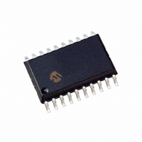
PIC16C781T-I/SO Microchip Technology, PIC16C781T-I/SO Datasheet - Page 19

PIC16C781T-I/SO
Manufacturer Part Number
PIC16C781T-I/SO
Description
IC MCU CMOS 8BIT 1K 20MHZ 20SOIC
Manufacturer
Microchip Technology
Series
PIC® 16Cr
Datasheets
1.PIC16C781-ISO.pdf
(186 pages)
2.PIC16C781-ISO.pdf
(8 pages)
3.PIC16C781-ISO.pdf
(8 pages)
Specifications of PIC16C781T-I/SO
Core Processor
PIC
Core Size
8-Bit
Speed
20MHz
Peripherals
Brown-out Detect/Reset, POR, PWM, WDT
Number Of I /o
13
Program Memory Size
1.75KB (1K x 14)
Program Memory Type
OTP
Ram Size
128 x 8
Voltage - Supply (vcc/vdd)
4 V ~ 5.5 V
Data Converters
A/D 8x8b; D/A 1x8b
Oscillator Type
Internal
Operating Temperature
-40°C ~ 85°C
Package / Case
20-SOIC (7.5mm Width)
For Use With
AC164028 - MODULE SKT PROMATEII 20SOIC/DIP
Lead Free Status / RoHS Status
Lead free / RoHS Compliant
Eeprom Size
-
Connectivity
-
Other names
PIC16C781TI/SO
- Current page: 19 of 186
- Download datasheet (4Mb)
2.3
The STATUS register, shown in Register 2-1, contains
the arithmetic status of the ALU, the RESET status and
the bank select bits for data memory.
The STATUS register can be the destination for any
instruction, as with any other register. If the STATUS
register is the destination for an instruction that affects
the Z, DC, or C bits, the write to these three bits is dis-
abled. These bits are set or cleared according to the
device logic. The TO and PD bits are not writable.
Therefore, the result of an instruction with the STATUS
register as the destination may be different than
intended.
REGISTER 2-1:
2001 Microchip Technology Inc.
STATUS Register
bit 7
bit 6-5
bit 4
bit 3
bit 2
bit 1
bit 0
STATUS REGISTER (STATUS: 03h, 83h, 103h, 183h)
Legend:
R = Readable bit
- n = Value at POR
IRP: Register Bank Select bit (used for indirect addressing)
1 = Bank 2, 3 (100h - 1FFh)
0 = Bank 0, 1 (00h - FFh)
RP<1:0>: Register Bank Select bits (used for direct addressing)
11 = Bank 3 (180h - 1FFh)
10 = Bank 2 (100h - 17Fh)
01 = Bank 1 (80h - FFh)
00 = Bank 0 (00h - 7Fh)
Each bank is 128 bytes
TO: Time-out bit
1 = After power-up, CLRWDT instruction, or SLEEP instruction
0 = A WDT time-out occurred
PD: Power-down bit
1 = After power-up or by the CLRWDT instruction
0 = By execution of the SLEEP instruction
Z: Zero bit
1 = The result of an arithmetic or logic operation is zero
0 = The result of an arithmetic or logic operation is not zero
DC: Digit carry/borrow bit (ADDWF, ADDLW,SUBLW,SUBWF instructions) (for borrow, the polarity
is reversed)
1 = A carry-out from the 4th low order bit of the result occurred
0 = No carry-out from the 4th low order bit of the result
C: Carry/borrow bit (ADDWF, ADDLW, SUBLW, SUBWF instructions)
1 = A carry-out from the Most Significant bit of the result occurred
0 = No carry-out from the Most Significant bit of the result occurred
bit7
R/W-0
Note:
IRP
For borrow, the polarity is reversed. A subtraction is executed by adding the two’s
complement of the second operand. For rotate (RRF, RLF) instructions, this bit is
loaded with either the high or low order bit of the source register.
R/W-0
RP1
R/W-0
RP0
Preliminary
W = Writable bit
’1’ = Bit is set
R-1
TO
For example, CLRF STATUS clears the upper three bits
and sets the Z bit. This leaves the STATUS register as
000u u1uu (where u = unchanged).
It is recommended, therefore, that only BCF, BSF,
SWAPF and MOVWF instructions are used to alter the
STATUS register, since these instructions do not affect
the Z, C, or DC bits from the STATUS register. For other
instructions not affecting any status bits, see the
"Instruction Set Summary."
Note:
R-1
PD
U = Unimplemented bit, read as ‘0’
’0’ = Bit is cleared
The C and DC bits operate as a borrow
and digit borrow bit, respectively, in sub-
traction. See the SUBLW and SUBWF
instructions for examples.
PIC16C781/782
R/W-x
Z
x = Bit is unknown
R/W-x
DC
DS41171A-page 17
R/W-x
C
bit0
Related parts for PIC16C781T-I/SO
Image
Part Number
Description
Manufacturer
Datasheet
Request
R

Part Number:
Description:
IC MCU OTP 1KX14 W/AD COMP20CDIP
Manufacturer:
Microchip Technology
Datasheet:

Part Number:
Description:
IC MCU OTP 1KX14 W/AD 20DIP
Manufacturer:
Microchip Technology
Datasheet:

Part Number:
Description:
IC MCU OTP 1KX14 W/AD COMP20SSOP
Manufacturer:
Microchip Technology
Datasheet:

Part Number:
Description:
IC MCU OTP 1KX14 W/AD 20SOIC
Manufacturer:
Microchip Technology
Datasheet:

Part Number:
Description:
IC MCU OTP 1KX14 W/AD 20SSOP
Manufacturer:
Microchip Technology
Datasheet:

Part Number:
Description:
IC MCU OTP 1KX14 W/AD COMP 20DIP
Manufacturer:
Microchip Technology
Datasheet:

Part Number:
Description:
1.75 KB OTP, 128 RAM, 16 I/O 20 SOIC .300in TUBE
Manufacturer:
Microchip Technology
Datasheet:

Part Number:
Description:
BOARD DEMO PICDEM FOR 16C781/782
Manufacturer:
Microchip Technology
Datasheet:

Part Number:
Description:
BOARD DEMO VOLTAGE BOOST MSC1
Manufacturer:
Microchip Technology
Datasheet:

Part Number:
Description:
BOARD DEMO DELTA SIGMA ADC MSC1
Manufacturer:
Microchip Technology
Datasheet:

Part Number:
Description:
IC, 8BIT MCU, PIC16C, 40MHZ, DIP-18
Manufacturer:
Microchip Technology
Datasheet:

Part Number:
Description:
IC, 8BIT MCU, PIC16C, 4MHZ, DIP-28
Manufacturer:
Microchip Technology
Datasheet:

Part Number:
Description:
IC, 8BIT MCU, PIC16C, 4MHZ, DIP-28
Manufacturer:
Microchip Technology
Datasheet:

Part Number:
Description:
IC, 8BIT MCU, PIC16C, 4MHZ, DIP-40
Manufacturer:
Microchip Technology
Datasheet:


