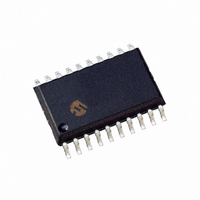
PIC16C781T-I/SO Microchip Technology, PIC16C781T-I/SO Datasheet - Page 72

PIC16C781T-I/SO
Manufacturer Part Number
PIC16C781T-I/SO
Description
IC MCU CMOS 8BIT 1K 20MHZ 20SOIC
Manufacturer
Microchip Technology
Series
PIC® 16Cr
Datasheets
1.PIC16C781-ISO.pdf
(186 pages)
2.PIC16C781-ISO.pdf
(8 pages)
3.PIC16C781-ISO.pdf
(8 pages)
Specifications of PIC16C781T-I/SO
Core Processor
PIC
Core Size
8-Bit
Speed
20MHz
Peripherals
Brown-out Detect/Reset, POR, PWM, WDT
Number Of I /o
13
Program Memory Size
1.75KB (1K x 14)
Program Memory Type
OTP
Ram Size
128 x 8
Voltage - Supply (vcc/vdd)
4 V ~ 5.5 V
Data Converters
A/D 8x8b; D/A 1x8b
Oscillator Type
Internal
Operating Temperature
-40°C ~ 85°C
Package / Case
20-SOIC (7.5mm Width)
For Use With
AC164028 - MODULE SKT PROMATEII 20SOIC/DIP
Lead Free Status / RoHS Status
Lead free / RoHS Compliant
Eeprom Size
-
Connectivity
-
Other names
PIC16C781TI/SO
- Current page: 72 of 186
- Download datasheet (4Mb)
PIC16C781/782
9.1
The ADC module has three registers. These registers
are:
• ADC Result Register:
• ADC Control Register 0:
• ADC Control Register 1:
The ADCON0 register, shown in Register 9-1, controls
the operations and input channel selection for the ADC
module. The ADCON1 register, shown in Register 9-3,
selects the voltage reference used by the ADC module.
The ADRES register, shown in Register 9-2, holds the
8-bit result of the conversion.
Additional information on using the ADC module can be
found in the PICmicro™ Mid-Range MCU Family Ref-
erence Manual (DS33023) and in Application Note
AN546 (DS00546).
REGISTER 9-1:
DS41171A-page 70
Control Registers
bit 7-6
bit 5-3
bit 2
bit 1
bit 0
ADC CONTROL REGISTER 0 (ADCON0: 1Fh)
bit 7
ADCS<1:0>: ADC Conversion Clock Select bits
00 = F
01 = F
10 = F
11 = ADRC (clock derived from a dedicated RC oscillator)
CHS<2:0>: Analog Channel Select bits (select which channel to convert)
If CHS3 = 0:
000 = channel 0 (AN0)
010 = channel 2 (AN2)
011 = channel 3 (AN3)
100 = channel 4 (AN4)
101 = channel 5 (AN5)
110 = channel 6 (AN6)
111 = channel 7 (AN7)
GO/DONE: ADC Conversion Status bit
1 = ADC conversion cycle in progress. Setting this bit starts an ADC conversion cycle.
0 = ADC conversion is not in progress (this bit is cleared by hardware when conversion is complete)
CHS3: Analog Channel Select bit
1 = Internal channel selected for conversion
0 = External channel selected for conversion
ADON: ADC On bit
1 = ADC enabled
0 = ADC disabled
Legend:
S = Settable bit
R = Readable bit
- n = Value at POR
001 = channel 1 (AN1)
ADCS1
R/W-0
ADRES
ADCON0
ADCON1
OSC
OSC
OSC
/2
/8
/32
ADCS0
R/W-0
R/W-0
CHS2
Preliminary
W = Writable bit
’1’ = Bit is set
R/W-0
CHS1
If CHS3 = 1:
000 = V
001 = V
010 = Reserved. Do not use.
011 = Reserved. Do not use.
100 = Reserved. Do not use.
101 = Reserved. Do not use.
110 = Reserved. Do not use.
111 = Reserved. Do not use.
9.1.1
The ADCON0 register, shown in Register 9-1, controls
the following:
• Clock source and prescaler
• Input channel
• Conversion start/stop
• Enabling of the ADC module
Setting the ADON bit, ADCON0<0>, enables the ADC
module. Clearing ADON disables the module and ter-
minates any conversion in process.
The ADCS<1:0> bits (ADCON0<7:6>) determine the
clock source used by the ADC module.
The CHS<3:0> bits (ADCON0<5:3,1>) determine the
input channel to the ADC module. CHS<3> specifically
determines whether the source is internal or external.
Setting the GO/DONE bit (ADCON0<2>) initiates the
conversion process. The ADC clears this bit at the
completion of the conversion process.
R
DAC
R/W-0
CHS0
U = Unimplemented bit, read as ‘0’
’0’ = Bit is cleared
ADCON0 REGISTER
GO/DONE
R/S-0
2001 Microchip Technology Inc.
x = Bit is unknown
R/W-0
CHS3
R/W-0
ADON
bit 0
Related parts for PIC16C781T-I/SO
Image
Part Number
Description
Manufacturer
Datasheet
Request
R

Part Number:
Description:
IC MCU OTP 1KX14 W/AD COMP20CDIP
Manufacturer:
Microchip Technology
Datasheet:

Part Number:
Description:
IC MCU OTP 1KX14 W/AD 20DIP
Manufacturer:
Microchip Technology
Datasheet:

Part Number:
Description:
IC MCU OTP 1KX14 W/AD COMP20SSOP
Manufacturer:
Microchip Technology
Datasheet:

Part Number:
Description:
IC MCU OTP 1KX14 W/AD 20SOIC
Manufacturer:
Microchip Technology
Datasheet:

Part Number:
Description:
IC MCU OTP 1KX14 W/AD 20SSOP
Manufacturer:
Microchip Technology
Datasheet:

Part Number:
Description:
IC MCU OTP 1KX14 W/AD COMP 20DIP
Manufacturer:
Microchip Technology
Datasheet:

Part Number:
Description:
1.75 KB OTP, 128 RAM, 16 I/O 20 SOIC .300in TUBE
Manufacturer:
Microchip Technology
Datasheet:

Part Number:
Description:
BOARD DEMO PICDEM FOR 16C781/782
Manufacturer:
Microchip Technology
Datasheet:

Part Number:
Description:
BOARD DEMO VOLTAGE BOOST MSC1
Manufacturer:
Microchip Technology
Datasheet:

Part Number:
Description:
BOARD DEMO DELTA SIGMA ADC MSC1
Manufacturer:
Microchip Technology
Datasheet:

Part Number:
Description:
IC, 8BIT MCU, PIC16C, 40MHZ, DIP-18
Manufacturer:
Microchip Technology
Datasheet:

Part Number:
Description:
IC, 8BIT MCU, PIC16C, 4MHZ, DIP-28
Manufacturer:
Microchip Technology
Datasheet:

Part Number:
Description:
IC, 8BIT MCU, PIC16C, 4MHZ, DIP-28
Manufacturer:
Microchip Technology
Datasheet:

Part Number:
Description:
IC, 8BIT MCU, PIC16C, 4MHZ, DIP-40
Manufacturer:
Microchip Technology
Datasheet:


