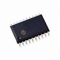
PIC16C781T-I/SO Microchip Technology, PIC16C781T-I/SO Datasheet - Page 83

PIC16C781T-I/SO
Manufacturer Part Number
PIC16C781T-I/SO
Description
IC MCU CMOS 8BIT 1K 20MHZ 20SOIC
Manufacturer
Microchip Technology
Series
PIC® 16Cr
Datasheets
1.PIC16C781-ISO.pdf
(186 pages)
2.PIC16C781-ISO.pdf
(8 pages)
3.PIC16C781-ISO.pdf
(8 pages)
Specifications of PIC16C781T-I/SO
Core Processor
PIC
Core Size
8-Bit
Speed
20MHz
Peripherals
Brown-out Detect/Reset, POR, PWM, WDT
Number Of I /o
13
Program Memory Size
1.75KB (1K x 14)
Program Memory Type
OTP
Ram Size
128 x 8
Voltage - Supply (vcc/vdd)
4 V ~ 5.5 V
Data Converters
A/D 8x8b; D/A 1x8b
Oscillator Type
Internal
Operating Temperature
-40°C ~ 85°C
Package / Case
20-SOIC (7.5mm Width)
For Use With
AC164028 - MODULE SKT PROMATEII 20SOIC/DIP
Lead Free Status / RoHS Status
Lead free / RoHS Compliant
Eeprom Size
-
Connectivity
-
Other names
PIC16C781TI/SO
- Current page: 83 of 186
- Download datasheet (4Mb)
10.3
Example 10-1 shows a sample configuration for the
DAC module. The port pin is configured, AV
selected for the voltage reference, and the DAC output
is enabled.
EXAMPLE 10-1:
;*
;*
;*
10.4
A device RESET forces all registers to their RESET
state. This forces the following conditions:
• DAC module is off
• Reference input to AV
• Output disabled
• DAC register is cleared
10.5
The accuracy/error specified for the DAC includes:
• Integral non-linearity error
• Differential non-linearity error
• Gain error
• Offset error
• Monotonicity
TABLE 10-1:
11Fh
11Eh
86h
9Dh
Legend: x = unknown, u = unchanged, - = unimplemented, read as '0'. Shaded cells are not used for DAC conversion.
Address
2001 Microchip Technology Inc.
This code block will configure the DAC
for AVDD Voltage Ref, and RB1/AN5/VDAC as
output.
BANKSEL TRISB
BSF
BSF
BANKSEL DACON0
CLRF
MOVLW
MOVWF
MOVLW
MOVWF
DAC Configuration
Effects of RESET
DAC Module Accuracy/Error
DACON0
DAC
TRISB
ANSEL
Name
TRISB,1
ANSEL,1
DAC
B’11000000’
DACON0
DAC_VALUE
DAC
REGISTERS/BITS ASSOCIATED WITH DAC
DAC CONFIGURATION
DAON
Bit 7
DD
DA7
RB7
AN7
; Select bank 1
; Set RB1 input
; Set RB1 as analog
; Select Bank 2
; DAC to 00
; Enable DAC output
; Set REF = VDD
; Set DAC output
DAOE
Bit 6
DA6
RB6
AN6
Bit 5
DA5
RB5
AN5
—
DD
Bit 4
DA4
RB4
AN4
Preliminary
—
is
Bit 3
DA3
RB3
AN3
—
FIGURE 10-2:
Offset error measures the first actual transition of a
code versus the first ideal transition of a code. Offset
error shifts the entire transfer function. Offset error can
be calibrated out of a system or introduced into a sys-
tem through the interaction of the output drive capabil-
ity with the load impedance.
Gain error measures the maximum deviation of the
last actual transition and the last ideal transition
adjusted for offset error. This error appears as a
change in slope of the transfer function. The difference
in gain error to full scale error is that full scale does not
take offset error into account. Gain error can be cali-
brated out by adjusting the reference voltage.
Linearity error refers to the uniformity of the voltage
change with code change. Linearity errors cannot be cal-
ibrated out of the system. Integral non-linearity error
measures the actual voltage output versus the ideal volt-
age output adjusted by the gain error for each code.
Differential non-linearity error measures the maxi-
mum actual voltage step versus the ideal voltage step.
This measure is unadjusted.
Bit 2
DA2
RB2
AN2
—
FEh
FFh
04h
03h
02h
01h
00h
DARS1 DARS0 00-- --00 00-- --00
Bit 1
DA1
RB1
AN1
PIC16C781/782
Bit 0
DA0
RB0
AN0
Analog Output Voltage
DAC TRANSFER
FUNCTION
0000 0000 0000 0000
1111 1111 1111 1111
1111 1111 1111 1111
Value on:
POR,
BOR
DS41171A-page 81
All Other
Value on
RESETS
Related parts for PIC16C781T-I/SO
Image
Part Number
Description
Manufacturer
Datasheet
Request
R

Part Number:
Description:
IC MCU OTP 1KX14 W/AD COMP20CDIP
Manufacturer:
Microchip Technology
Datasheet:

Part Number:
Description:
IC MCU OTP 1KX14 W/AD 20DIP
Manufacturer:
Microchip Technology
Datasheet:

Part Number:
Description:
IC MCU OTP 1KX14 W/AD COMP20SSOP
Manufacturer:
Microchip Technology
Datasheet:

Part Number:
Description:
IC MCU OTP 1KX14 W/AD 20SOIC
Manufacturer:
Microchip Technology
Datasheet:

Part Number:
Description:
IC MCU OTP 1KX14 W/AD 20SSOP
Manufacturer:
Microchip Technology
Datasheet:

Part Number:
Description:
IC MCU OTP 1KX14 W/AD COMP 20DIP
Manufacturer:
Microchip Technology
Datasheet:

Part Number:
Description:
1.75 KB OTP, 128 RAM, 16 I/O 20 SOIC .300in TUBE
Manufacturer:
Microchip Technology
Datasheet:

Part Number:
Description:
BOARD DEMO PICDEM FOR 16C781/782
Manufacturer:
Microchip Technology
Datasheet:

Part Number:
Description:
BOARD DEMO VOLTAGE BOOST MSC1
Manufacturer:
Microchip Technology
Datasheet:

Part Number:
Description:
BOARD DEMO DELTA SIGMA ADC MSC1
Manufacturer:
Microchip Technology
Datasheet:

Part Number:
Description:
IC, 8BIT MCU, PIC16C, 40MHZ, DIP-18
Manufacturer:
Microchip Technology
Datasheet:

Part Number:
Description:
IC, 8BIT MCU, PIC16C, 4MHZ, DIP-28
Manufacturer:
Microchip Technology
Datasheet:

Part Number:
Description:
IC, 8BIT MCU, PIC16C, 4MHZ, DIP-28
Manufacturer:
Microchip Technology
Datasheet:

Part Number:
Description:
IC, 8BIT MCU, PIC16C, 4MHZ, DIP-40
Manufacturer:
Microchip Technology
Datasheet:


