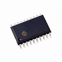
PIC16C781T-I/SO Microchip Technology, PIC16C781T-I/SO Datasheet - Page 78

PIC16C781T-I/SO
Manufacturer Part Number
PIC16C781T-I/SO
Description
IC MCU CMOS 8BIT 1K 20MHZ 20SOIC
Manufacturer
Microchip Technology
Series
PIC® 16Cr
Datasheets
1.PIC16C781-ISO.pdf
(186 pages)
2.PIC16C781-ISO.pdf
(8 pages)
3.PIC16C781-ISO.pdf
(8 pages)
Specifications of PIC16C781T-I/SO
Core Processor
PIC
Core Size
8-Bit
Speed
20MHz
Peripherals
Brown-out Detect/Reset, POR, PWM, WDT
Number Of I /o
13
Program Memory Size
1.75KB (1K x 14)
Program Memory Type
OTP
Ram Size
128 x 8
Voltage - Supply (vcc/vdd)
4 V ~ 5.5 V
Data Converters
A/D 8x8b; D/A 1x8b
Oscillator Type
Internal
Operating Temperature
-40°C ~ 85°C
Package / Case
20-SOIC (7.5mm Width)
For Use With
AC164028 - MODULE SKT PROMATEII 20SOIC/DIP
Lead Free Status / RoHS Status
Lead free / RoHS Compliant
Eeprom Size
-
Connectivity
-
Other names
PIC16C781TI/SO
- Current page: 78 of 186
- Download datasheet (4Mb)
PIC16C781/782
9.6.1
In systems where the device frequency is low, use of
the ADC RC clock is preferred. At moderate to high fre-
quencies, T
lator. T
when derived from T
phase clock transitions. This reduces, to a large extent,
the effects of digital switching noise. This is not possi-
ble with the RC derived clock. The loss of accuracy due
to digital switching noise can be significant if many I/O
pins are active.
In systems where the device enters SLEEP mode after
the start of the ADC conversion, the RC clock source
selection is required. In this mode, the digital noise
from the modules in SLEEP is stopped. This method
gives high accuracy.
9.7
A device RESET forces all registers to their RESET
state. This forces the ADC module to be turned off, and
any conversion is aborted.
The value that is in the ADRES register is not modified
for a Power-on Reset. The ADRES register contains
unknown data after a Power-on Reset.
9.8
If the input voltage exceeds the rail values (V
by greater than 0.2V, then the accuracy of the conver-
sion is out of specification.
An external RC filter is sometimes added for anti-
aliasing of the input signal. The R component should be
selected to ensure that the total source impedance is
kept under the 10 k recommended specification. Any
external components connected (via hi-impedance) to
an analog input pin (capacitor, zener diode, etc.) should
have very little leakage current at the pin.
DS41171A-page 76
8 s for preferred operation. This is because T
Note:
AD
Effects of a RESET
Connection Considerations
must not violate the minimum and should be
Care must be taken when using the RB2/
AN6 pin in ADC conversions due to its
proximity to the OSC1 pin.
AD
CLOCK NOISE
should be derived from the device oscil-
OSC
, is kept away from on-chip
SS
or V
Preliminary
DD
AD
)
,
9.9
The ideal transfer function of the ADC converter is as
follows: the first transition occurs when the analog input
voltage (V
9.10
A good reference for ADC converters is the "Analog-
Digital Conversion Handbook" third edition, published
by Prentice Hall (ISBN 0-13-03-2848-0).
FIGURE 9-3:
FEh
FFh
04h
03h
02h
01h
00h
Transfer Function
References
AIN
) is Analog ADC
Analog Input Voltage
ADC TRANSFER
FUNCTION
2001 Microchip Technology Inc.
REF
/256 (Figure 9-3).
Related parts for PIC16C781T-I/SO
Image
Part Number
Description
Manufacturer
Datasheet
Request
R

Part Number:
Description:
IC MCU OTP 1KX14 W/AD COMP20CDIP
Manufacturer:
Microchip Technology
Datasheet:

Part Number:
Description:
IC MCU OTP 1KX14 W/AD 20DIP
Manufacturer:
Microchip Technology
Datasheet:

Part Number:
Description:
IC MCU OTP 1KX14 W/AD COMP20SSOP
Manufacturer:
Microchip Technology
Datasheet:

Part Number:
Description:
IC MCU OTP 1KX14 W/AD 20SOIC
Manufacturer:
Microchip Technology
Datasheet:

Part Number:
Description:
IC MCU OTP 1KX14 W/AD 20SSOP
Manufacturer:
Microchip Technology
Datasheet:

Part Number:
Description:
IC MCU OTP 1KX14 W/AD COMP 20DIP
Manufacturer:
Microchip Technology
Datasheet:

Part Number:
Description:
1.75 KB OTP, 128 RAM, 16 I/O 20 SOIC .300in TUBE
Manufacturer:
Microchip Technology
Datasheet:

Part Number:
Description:
BOARD DEMO PICDEM FOR 16C781/782
Manufacturer:
Microchip Technology
Datasheet:

Part Number:
Description:
BOARD DEMO VOLTAGE BOOST MSC1
Manufacturer:
Microchip Technology
Datasheet:

Part Number:
Description:
BOARD DEMO DELTA SIGMA ADC MSC1
Manufacturer:
Microchip Technology
Datasheet:

Part Number:
Description:
IC, 8BIT MCU, PIC16C, 40MHZ, DIP-18
Manufacturer:
Microchip Technology
Datasheet:

Part Number:
Description:
IC, 8BIT MCU, PIC16C, 4MHZ, DIP-28
Manufacturer:
Microchip Technology
Datasheet:

Part Number:
Description:
IC, 8BIT MCU, PIC16C, 4MHZ, DIP-28
Manufacturer:
Microchip Technology
Datasheet:

Part Number:
Description:
IC, 8BIT MCU, PIC16C, 4MHZ, DIP-40
Manufacturer:
Microchip Technology
Datasheet:


