ATXMEGA16A4-CUR Atmel, ATXMEGA16A4-CUR Datasheet - Page 232
ATXMEGA16A4-CUR
Manufacturer Part Number
ATXMEGA16A4-CUR
Description
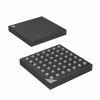
MCU AVR 16+4KB FLASH 49VFBGA
Manufacturer
Atmel
Series
AVR® XMEGAr
Specifications of ATXMEGA16A4-CUR
Core Processor
AVR
Core Size
8/16-Bit
Speed
32MHz
Connectivity
I²C, IrDA, SPI, UART/USART
Peripherals
Brown-out Detect/Reset, DMA, POR, PWM, WDT
Number Of I /o
34
Program Memory Size
16KB (8K x 16)
Program Memory Type
FLASH
Eeprom Size
1K x 8
Ram Size
2K x 8
Voltage - Supply (vcc/vdd)
1.6 V ~ 3.6 V
Data Converters
A/D 12x12b, D/A 2x12b
Oscillator Type
Internal
Operating Temperature
-40°C ~ 85°C
Package / Case
49-VFBGA
For Use With
ATAVRONEKIT - KIT AVR/AVR32 DEBUGGER/PROGRMMRATSTK600 - DEV KIT FOR AVR/AVR32770-1007 - ISP 4PORT ATMEL AVR MCU SPI/JTAG770-1004 - ISP 4PORT FOR ATMEL AVR MCU SPI
Lead Free Status / RoHS Status
Lead free / RoHS Compliant
Available stocks
Company
Part Number
Manufacturer
Quantity
Price


20.6
20.7
20.7.1
8077H–AVR–12/09
DMA Support
Register Description
CTRL - SPI Control Register
DMA support on the SPI module is only available in Slave mode. The SPI Slave can trigger a
DMA transfer as one byte has been shifted into the Data Register. It is possible to set up the
XMEGA USART in SPI mode to have DMA support for master mode, for details refer to
21.10 ”USART in Master SPI Mode” on page
• Bit 7 - CLK2X: SPI Clock Double
When this bit is set the SPI speed (SCK Frequency) will be doubled in Master mode (see
20-4 on page
• Bit 6 - ENABLE: SPI Enable
Setting this bit enables the SPI modules. This bit must be set to enable any SPI operations.
• Bit 5 - DORD: Data Order
DORD decide the data order when a byte is shifted out from the Data register. When DORD is
written to one, the LSB of the data byte is transmitted first, and when DORD is written to zero,
the MSB of the data byte is transmitted first.
• Bit 4 - MASTER: Master/Slave Select
This bit selects Master mode when written to one, and Slave mode when written to zero. If SS is
configured as an input and is driven low while MASTER is set, MASTER will be cleared.
• Bit 3:2 - MODE[1:0]: SPI Mode
These bits select the transfer mode. The four combinations of SCK phase and polarity with
respect to serial data is shown in
a clock cycles (leading edge) is rising or falling, and if data setup and sample is on lading or trail-
ing edge.
When the leading edge is rising the bit SCK is low when idle, and when the leading edge is fall-
ing the SCK is high when idle.
Table 20-3.
Bit
+0x00
Read/Write
Initial Value
MODE[1:0]
00
01
10
11
CLK2X
R/W
233).
7
0
SPI transfer modes
ENABLE
Group Configuration
R/W
6
0
0
1
2
3
DORD
R/W
5
0
Figure 20-3 on page
MASTER
R/W
4
0
247.
Rising, Sample
Leading Edge
Falling,Sample
Rising, Setup
Falling, Setup
R/W
3
0
MODE[1:0]
232. This decide whether the first edge in
R/W
2
0
R/W
PRESCALER[1:0]
1
0
Falling, Sample
Rising, Sample
Trailing Edge
Falling, Setup
Rising, Setup
XMEGA A
R/W
0
0
Section
CTRL
Table
232
Related parts for ATXMEGA16A4-CUR
Image
Part Number
Description
Manufacturer
Datasheet
Request
R

Part Number:
Description:
DEV KIT FOR AVR/AVR32
Manufacturer:
Atmel
Datasheet:

Part Number:
Description:
INTERVAL AND WIPE/WASH WIPER CONTROL IC WITH DELAY
Manufacturer:
ATMEL Corporation
Datasheet:
Part Number:
Description:
Low-Voltage Voice-Switched IC for Hands-Free Operation
Manufacturer:
ATMEL Corporation
Datasheet:
Part Number:
Description:
MONOLITHIC INTEGRATED FEATUREPHONE CIRCUIT
Manufacturer:
ATMEL Corporation
Datasheet:
Part Number:
Description:
AM-FM Receiver IC U4255BM-M
Manufacturer:
ATMEL Corporation
Datasheet:
Part Number:
Description:
Monolithic Integrated Feature Phone Circuit
Manufacturer:
ATMEL Corporation
Datasheet:
Part Number:
Description:
Multistandard Video-IF and Quasi Parallel Sound Processing
Manufacturer:
ATMEL Corporation
Datasheet:
Part Number:
Description:
High-performance EE PLD
Manufacturer:
ATMEL Corporation
Datasheet:
Part Number:
Description:
8-bit Flash Microcontroller
Manufacturer:
ATMEL Corporation
Datasheet:
Part Number:
Description:
2-Wire Serial EEPROM
Manufacturer:
ATMEL Corporation
Datasheet: