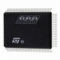
ST92F150CV1QB STMicroelectronics, ST92F150CV1QB Datasheet - Page 142

ST92F150CV1QB
Manufacturer Part Number
ST92F150CV1QB
Description
MCU 8BIT 128K FLASH 100PQFP
Manufacturer
STMicroelectronics
Series
ST9r
Datasheet
1.ST92F150CV1TB.pdf
(429 pages)
Specifications of ST92F150CV1QB
Core Processor
ST9
Core Size
8/16-Bit
Speed
24MHz
Connectivity
CAN, I²C, LIN, SCI, SPI
Peripherals
DMA, LVD, POR, PWM, WDT
Number Of I /o
77
Program Memory Size
128KB (128K x 8)
Program Memory Type
FLASH
Eeprom Size
1K x 8
Ram Size
4K x 8
Voltage - Supply (vcc/vdd)
4.5 V ~ 5.5 V
Data Converters
A/D 16x10b
Oscillator Type
Internal
Operating Temperature
-40°C ~ 105°C
Package / Case
100-QFP
Processor Series
ST92F15x
Core
ST9
Data Bus Width
8 bit, 16 bit
Data Ram Size
6 KB
Interface Type
CAN, I2C, SCI, SPI
Maximum Clock Frequency
24 MHz
Number Of Programmable I/os
80
Number Of Timers
5 x 16 bit
Operating Supply Voltage
4.5 V to 5.5 V
Maximum Operating Temperature
+ 105 C
Mounting Style
SMD/SMT
Development Tools By Supplier
ST92F150-EPB
Minimum Operating Temperature
- 40 C
On-chip Adc
16 bit x 10 bit
Lead Free Status / RoHS Status
Lead free / RoHS Compliant
Other names
497-4882
Available stocks
Company
Part Number
Manufacturer
Quantity
Price
Company:
Part Number:
ST92F150CV1QB
Manufacturer:
STMicroelectronics
Quantity:
10 000
- Current page: 142 of 429
- Download datasheet (8Mb)
ST92F124/F150/F250 - EXTERNAL MEMORY INTERFACE (EXTMI)
8 EXTERNAL MEMORY INTERFACE (EXTMI)
8.1 INTRODUCTION
The ST9 External Memory Interface uses two reg-
isters (EMR1 and EMR2) to configure external
memory accesses. Some interface signals are
also affected by WCR - R252 Page 0.
If the two registers EMR1 and EMR2 are set to the
proper values, the ST9+ memory access cycle is
similar to that of the original ST9, with the only ex-
ception that it is composed of just two system
clock phases, named T1 and T2.
During phase T1, the memory address is output on
the AS falling edge and is valid on the rising edge
of AS. Port1 and Port 9 maintain the address sta-
ble until the following T1 phase.
Figure 73. Page 21 Registers
142/429
9
FFh
FEh
FDh
FCh
FBh
FAh
F9h
F8h
F7h
F6h
F5h
F4h
F3h
F2h
F1h
F0h
Page 21
DMASR
ISR
EMR2
EMR1
CSR
DPR3
DPR2
DPR1
DPR0
R255
R254
R253
R252
R251
R250
R249
R248
R247
R246
R245
R244
R243
R242
R241
R240
MMU
EXT.MEM
MMU
MODER
FLAGR
USPH
SSPH
SSPL
USPL
CICR
PPR
RP1
RP0
P5
P4
P3
P2
P1
P0
Bit DPRREM=0
Relocation of P0-3 and DPR0-3 Registers
During phase T2, two forms of behavior are possi-
ble. If the memory access is a Read cycle, Port 0
pins are released in high-impedance until the next
T1 phase and the data signals are sampled by the
ST9 on the rising edge of DS. If the memory ac-
cess is a Write cycle, on the falling edge of DS,
Port 0 outputs data to be written in the external
memory. Those data signals are valid on the rising
edge of DS and are maintained stable until the
next address is output.
Note that DS is pulled low at the beginning of
phase T2 only during an external memory access.
DMASR
EMR2
EMR1
DPR3
DPR2
DPR1
DPR0
CSR
ISR
MODER
FLAGR
SSPH
USPH
USPL
DPR3
DPR2
DPR1
DPR0
SSPL
CICR
PPR
RP1
RP0
P5
P4
Bit DPRREM=1
DMASR
EMR2
EMR1
CSR
ISR
P3
P2
P1
P0
Related parts for ST92F150CV1QB
Image
Part Number
Description
Manufacturer
Datasheet
Request
R

Part Number:
Description:
BOARD PROGRAM FOR ST92F150 MCU
Manufacturer:
STMicroelectronics
Datasheet:

Part Number:
Description:
BOARD EVALUATION FOR ST9 SERIES
Manufacturer:
STMicroelectronics
Datasheet:

Part Number:
Description:
BOARD EMULATOR FOR ST9 SERIES
Manufacturer:
STMicroelectronics
Datasheet:

Part Number:
Description:
MCU, MPU & DSP Development Tools ST9 Dedication Board
Manufacturer:
STMicroelectronics
Datasheet:

Part Number:
Description:
STMicroelectronics [RIPPLE-CARRY BINARY COUNTER/DIVIDERS]
Manufacturer:
STMicroelectronics
Datasheet:

Part Number:
Description:
STMicroelectronics [LIQUID-CRYSTAL DISPLAY DRIVERS]
Manufacturer:
STMicroelectronics
Datasheet:

Part Number:
Description:
BOARD EVAL FOR MEMS SENSORS
Manufacturer:
STMicroelectronics
Datasheet:

Part Number:
Description:
NPN TRANSISTOR POWER MODULE
Manufacturer:
STMicroelectronics
Datasheet:

Part Number:
Description:
TURBOSWITCH ULTRA-FAST HIGH VOLTAGE DIODE
Manufacturer:
STMicroelectronics
Datasheet:

Part Number:
Description:
Manufacturer:
STMicroelectronics
Datasheet:

Part Number:
Description:
DIODE / SCR MODULE
Manufacturer:
STMicroelectronics
Datasheet:

Part Number:
Description:
DIODE / SCR MODULE
Manufacturer:
STMicroelectronics
Datasheet:


