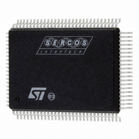
ST92F150CV1QB STMicroelectronics, ST92F150CV1QB Datasheet - Page 419

ST92F150CV1QB
Manufacturer Part Number
ST92F150CV1QB
Description
MCU 8BIT 128K FLASH 100PQFP
Manufacturer
STMicroelectronics
Series
ST9r
Datasheet
1.ST92F150CV1TB.pdf
(429 pages)
Specifications of ST92F150CV1QB
Core Processor
ST9
Core Size
8/16-Bit
Speed
24MHz
Connectivity
CAN, I²C, LIN, SCI, SPI
Peripherals
DMA, LVD, POR, PWM, WDT
Number Of I /o
77
Program Memory Size
128KB (128K x 8)
Program Memory Type
FLASH
Eeprom Size
1K x 8
Ram Size
4K x 8
Voltage - Supply (vcc/vdd)
4.5 V ~ 5.5 V
Data Converters
A/D 16x10b
Oscillator Type
Internal
Operating Temperature
-40°C ~ 105°C
Package / Case
100-QFP
Processor Series
ST92F15x
Core
ST9
Data Bus Width
8 bit, 16 bit
Data Ram Size
6 KB
Interface Type
CAN, I2C, SCI, SPI
Maximum Clock Frequency
24 MHz
Number Of Programmable I/os
80
Number Of Timers
5 x 16 bit
Operating Supply Voltage
4.5 V to 5.5 V
Maximum Operating Temperature
+ 105 C
Mounting Style
SMD/SMT
Development Tools By Supplier
ST92F150-EPB
Minimum Operating Temperature
- 40 C
On-chip Adc
16 bit x 10 bit
Lead Free Status / RoHS Status
Lead free / RoHS Compliant
Other names
497-4882
Available stocks
Company
Part Number
Manufacturer
Quantity
Price
Company:
Part Number:
ST92F150CV1QB
Manufacturer:
STMicroelectronics
Quantity:
10 000
- Current page: 419 of 429
- Download datasheet (8Mb)
KNOWN LIMITATIONS (Cont’d)
13.7 MFT DMA MASK BIT RESET WHEN MFT0
DMA PRIORITY LEVEL IS SET TO 0
Introduction
The MultiFunction Timer is a 16-bit timer with Input
Capture and Output Compare modes. In Input
Capture mode, the timer value is saved when an
external event occurs. In Output Compare mode,
the timer changes an I/O pin level when it reaches
the Compare Register value.
In these two modes the event (Input Capture or
Output Compare) may generate an interrupt or re-
quest a Direct Memory Access.
– In interrupt Input Capture mode (or Output Com-
– In DMA mode these transfers are done automat-
The choice between Interrupt or DMA modes is
defined by the CP0D and CM0D bits (bit 6 and bit
3 in the IDMR register, R255 page 10/8).
CP0D : Capture 0 DMA Mask. Capture on REG0R
DMA is enabled when CP0D = 1.
CM0D: Compare 0 DMA Mask. Compare on
CMP0R DMA is enabled when CM0D = 1.
In DMA mode a DMA counter register and a DMA
address register define the location and the size of
pare mode), the interrupt routine saves the coun-
ter in the RAM or the Register File (or updates
the compare register from a location in RAM or
in the Register File).
ically.
ST92F124/F150/F250 - KNOWN LIMITATIONS
the memory block (RAM or Reg. File) involved in
these transfers.
Each DMA transfer decreases the counter value.
When the counter reaches 0, an EndOfBlock
event occurs on the DMA controller. This event is
detected by the MFT which resets the CP0D or the
CM0D bit.
Limitation Description
The MFT1 resets its DMA Mask bit even if the
End-of-Block signal is dedicated to the MFT0.
This limitation occurs if the following conditions are
fulfilled:
– a MFT DMA request (for instance MFT1) occurs
– the MFT0 DMA request corresponds to an End-
– the MFT0 DMA priority level is set to 0.
This limitation is due to wrong End-of-Block event
management by the MFT, it does not impact the
SCI and the I2C but they can be involved in the
limitation if:
– First peripheral requests a DMA transfer with
– Other peripherals request a DMA transfer with a
End-of-Block event,
higher priority level between the same two DMA
arbitrations. As a consequence, the MFT1 DMA
request is not serviced and a DMA transfer is
lost. This is also true for a Top Level Interrupt
(higher priority than DMA).
while another peripheral DMA request is being
serviced (for instance MFT0),
of-Block
419/429
1
Related parts for ST92F150CV1QB
Image
Part Number
Description
Manufacturer
Datasheet
Request
R

Part Number:
Description:
BOARD PROGRAM FOR ST92F150 MCU
Manufacturer:
STMicroelectronics
Datasheet:

Part Number:
Description:
BOARD EVALUATION FOR ST9 SERIES
Manufacturer:
STMicroelectronics
Datasheet:

Part Number:
Description:
BOARD EMULATOR FOR ST9 SERIES
Manufacturer:
STMicroelectronics
Datasheet:

Part Number:
Description:
MCU, MPU & DSP Development Tools ST9 Dedication Board
Manufacturer:
STMicroelectronics
Datasheet:

Part Number:
Description:
STMicroelectronics [RIPPLE-CARRY BINARY COUNTER/DIVIDERS]
Manufacturer:
STMicroelectronics
Datasheet:

Part Number:
Description:
STMicroelectronics [LIQUID-CRYSTAL DISPLAY DRIVERS]
Manufacturer:
STMicroelectronics
Datasheet:

Part Number:
Description:
BOARD EVAL FOR MEMS SENSORS
Manufacturer:
STMicroelectronics
Datasheet:

Part Number:
Description:
NPN TRANSISTOR POWER MODULE
Manufacturer:
STMicroelectronics
Datasheet:

Part Number:
Description:
TURBOSWITCH ULTRA-FAST HIGH VOLTAGE DIODE
Manufacturer:
STMicroelectronics
Datasheet:

Part Number:
Description:
Manufacturer:
STMicroelectronics
Datasheet:

Part Number:
Description:
DIODE / SCR MODULE
Manufacturer:
STMicroelectronics
Datasheet:

Part Number:
Description:
DIODE / SCR MODULE
Manufacturer:
STMicroelectronics
Datasheet:


