ST92F150CV1QB STMicroelectronics, ST92F150CV1QB Datasheet - Page 318
ST92F150CV1QB
Manufacturer Part Number
ST92F150CV1QB
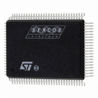
Description
MCU 8BIT 128K FLASH 100PQFP
Manufacturer
STMicroelectronics
Series
ST9r
Datasheet
1.ST92F150CV1TB.pdf
(429 pages)
Specifications of ST92F150CV1QB
Core Processor
ST9
Core Size
8/16-Bit
Speed
24MHz
Connectivity
CAN, I²C, LIN, SCI, SPI
Peripherals
DMA, LVD, POR, PWM, WDT
Number Of I /o
77
Program Memory Size
128KB (128K x 8)
Program Memory Type
FLASH
Eeprom Size
1K x 8
Ram Size
4K x 8
Voltage - Supply (vcc/vdd)
4.5 V ~ 5.5 V
Data Converters
A/D 16x10b
Oscillator Type
Internal
Operating Temperature
-40°C ~ 105°C
Package / Case
100-QFP
Processor Series
ST92F15x
Core
ST9
Data Bus Width
8 bit, 16 bit
Data Ram Size
6 KB
Interface Type
CAN, I2C, SCI, SPI
Maximum Clock Frequency
24 MHz
Number Of Programmable I/os
80
Number Of Timers
5 x 16 bit
Operating Supply Voltage
4.5 V to 5.5 V
Maximum Operating Temperature
+ 105 C
Mounting Style
SMD/SMT
Development Tools By Supplier
ST92F150-EPB
Minimum Operating Temperature
- 40 C
On-chip Adc
16 bit x 10 bit
Lead Free Status / RoHS Status
Lead free / RoHS Compliant
Other names
497-4882
Available stocks
Company
Part Number
Manufacturer
Quantity
Price
Company:

Part Number:
ST92F150CV1QB
Manufacturer:
STMicroelectronics
Quantity:
10 000


J1850 Byte Level Protocol Decoder (JBLPD)
J1850 BYTE LEVEL PROTOCOL DECODER (Cont’d)
Bit 5 = RDRF_M Receive Data Register Full Inter-
rupt Mask bit.
This bit enables the “receive data register full” in-
terrupt source to generate an interrupt request.
This bit is reset if the CONTROL.JDIS bit is set at
least for 6 clock cycles (3 NOPs).
0: RDRF interrupt source masked
1: RDRF interrupt source un-masked
Bit 4 = TLA_M Transmitter Lost Arbitration Inter-
rupt Mask bit.
This bit enables the “transmitter lost arbitration” in-
terrupt source to generate an interrupt request.
This bit is reset if the CONTROL.JDIS bit is set at
least for 6 clock cycles (3 NOPs).
0: TLA interrupt source masked
1: TLA interrupt source un-masked
Bit 3 = RXD_M Receiver DMA Mask bit.
If this bit is “0” no receiver DMA request will be
generated, and the RDRF bit, in the Status Regis-
ter (STATUS), can request an interrupt. If RXD_M
bit is set to “1” then the RDRF bit can request a
DMA transfer. RXD_M is reset by hardware when
the transaction counter value decrements to zero,
that is when a Receiver End Of Block condition oc-
curs (REOBP flag set).
This bit is reset if the CONTROL.JDIS bit is set at
least for 6 clock cycles (3 NOPs).
0: Receiver DMA disabled
1: Receiver DMA enabled
Bit 2 = EODM_M End of Data Minimum Interrupt
Mask bit.
This bit enables the “end of data minimum” inter-
rupt source to generate an interrupt request.
This bit is reset if the CONTROL.JDIS bit is set at
least for 6 clock cycles (3 NOPs).
0: EODM interrupt source mask
1: EODM interrupt source un-masked
Bit 1 = EOFM_M End of Frame Minimum Interrupt
Mask bit.
This bit enables the “end of frame minimum” inter-
rupt source to generate an interrupt request.
This bit is reset if the CONTROL.JDIS bit is set at
least for 6 clock cycles (3 NOPs).
0: EOFM interrupt source masked
1: EOFM interrupt source un-masked
318/429
9
Bit 0 = TXD_M Transmitter DMA Mask bit.
If this bit is “0” no transmitter DMA request will be
generated, and the TRDY bit, in the Status Regis-
ter (STATUS), can request an interrupt. If TXD_M
bit is set to “1” then the TRDY bit can request a
DMA transfer. TXD_M is reset by hardware when
the transaction counter value decrements to zero,
that is when a Transmitter End Of Block condition
occurs (TEOBP flag set).
This bit is reset if the CONTROL.JDIS bit is set at
least for 6 clock cycles (3 NOPs).
0: Transmitter DMA disabled
1: Transmitter DMA enabled
JBLPD OPTIONS AND REGISTER GROUPS
SELECTION REGISTER (OPTIONS)
R251- Read/Write
Register Page: 23
Reset Value: 0000 0000 (00h)
Bit 7 = INPOL VPWI Input Polarity Selector.
This bit allows the selection of the polarity of the
RX signal coming from the transceivers. Depend-
ing on the specific transceiver, the RX signal is in-
verted or not inverted respect the VPWO and the
J1850 bus line.
0: VPWI input is inverted by the transceiver with
1: VPWI input is not inverted by the transceiver
Bit 6 = NBSYMS NB Symbol Form Selector.
This bit allows the selection of the form of the Nor-
malization Bits (NB0/NB1).
0: NB0 active long symbol (Tv2), NB1 active short
1: NB0 active short symbol (Tv1), NB1 active long
INPOL NBSYMS DMASUSP LOOPB RSEL3 RSEL2 RSEL1 RSEL0
7
respect to the J1850 line.
with respect to the J1850 line.
symbol (Tv1)
symbol (Tv2)
0
Related parts for ST92F150CV1QB
Image
Part Number
Description
Manufacturer
Datasheet
Request
R

Part Number:
Description:
BOARD PROGRAM FOR ST92F150 MCU
Manufacturer:
STMicroelectronics
Datasheet:
Part Number:
Description:
BOARD EVALUATION FOR ST9 SERIES
Manufacturer:
STMicroelectronics
Datasheet:
Part Number:
Description:
BOARD EMULATOR FOR ST9 SERIES
Manufacturer:
STMicroelectronics
Datasheet:
Part Number:
Description:
MCU, MPU & DSP Development Tools ST9 Dedication Board
Manufacturer:
STMicroelectronics
Datasheet:
Part Number:
Description:
STMicroelectronics [RIPPLE-CARRY BINARY COUNTER/DIVIDERS]
Manufacturer:
STMicroelectronics
Datasheet:
Part Number:
Description:
STMicroelectronics [LIQUID-CRYSTAL DISPLAY DRIVERS]
Manufacturer:
STMicroelectronics
Datasheet:

Part Number:
Description:
BOARD EVAL FOR MEMS SENSORS
Manufacturer:
STMicroelectronics
Datasheet:
Part Number:
Description:
NPN TRANSISTOR POWER MODULE
Manufacturer:
STMicroelectronics
Datasheet:
Part Number:
Description:
TURBOSWITCH ULTRA-FAST HIGH VOLTAGE DIODE
Manufacturer:
STMicroelectronics
Datasheet:
Part Number:
Description:
Manufacturer:
STMicroelectronics
Datasheet:
Part Number:
Description:
DIODE / SCR MODULE
Manufacturer:
STMicroelectronics
Datasheet:
Part Number:
Description:
DIODE / SCR MODULE
Manufacturer:
STMicroelectronics
Datasheet: