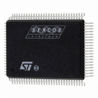
ST92F150CV1QB STMicroelectronics, ST92F150CV1QB Datasheet - Page 155

ST92F150CV1QB
Manufacturer Part Number
ST92F150CV1QB
Description
MCU 8BIT 128K FLASH 100PQFP
Manufacturer
STMicroelectronics
Series
ST9r
Datasheet
1.ST92F150CV1TB.pdf
(429 pages)
Specifications of ST92F150CV1QB
Core Processor
ST9
Core Size
8/16-Bit
Speed
24MHz
Connectivity
CAN, I²C, LIN, SCI, SPI
Peripherals
DMA, LVD, POR, PWM, WDT
Number Of I /o
77
Program Memory Size
128KB (128K x 8)
Program Memory Type
FLASH
Eeprom Size
1K x 8
Ram Size
4K x 8
Voltage - Supply (vcc/vdd)
4.5 V ~ 5.5 V
Data Converters
A/D 16x10b
Oscillator Type
Internal
Operating Temperature
-40°C ~ 105°C
Package / Case
100-QFP
Processor Series
ST92F15x
Core
ST9
Data Bus Width
8 bit, 16 bit
Data Ram Size
6 KB
Interface Type
CAN, I2C, SCI, SPI
Maximum Clock Frequency
24 MHz
Number Of Programmable I/os
80
Number Of Timers
5 x 16 bit
Operating Supply Voltage
4.5 V to 5.5 V
Maximum Operating Temperature
+ 105 C
Mounting Style
SMD/SMT
Development Tools By Supplier
ST92F150-EPB
Minimum Operating Temperature
- 40 C
On-chip Adc
16 bit x 10 bit
Lead Free Status / RoHS Status
Lead free / RoHS Compliant
Other names
497-4882
Available stocks
Company
Part Number
Manufacturer
Quantity
Price
Company:
Part Number:
ST92F150CV1QB
Manufacturer:
STMicroelectronics
Quantity:
10 000
- Current page: 155 of 429
- Download datasheet (8Mb)
INPUT/OUTPUT BIT CONFIGURATION (Cont’d)
When Px.n is programmed as an Output:
(Figure
– The Output Buffer is turned on in an Open-drain
– The data stored in the Output Master Latch is
When Px.n is programmed as Bidirectional:
(Figure
– The Output Buffer is turned on in an Open-Drain
– The data present on the I/O pin is sampled into
– The data stored in the Output Master Latch is
WARNING: Due to the fact that in bidirectional
mode the external pin is read instead of the output
latch, particular care must be taken with arithme-
tic/logic and Boolean instructions performed on a
bidirectional port pin.
These instructions use a read-modify-write se-
quence, and the result written in the port register
depends on the logical level present on the exter-
nal pin.
This may bring unwanted modifications to the port
output register content.
For example:
Port register content, 0Fh
external port value, 03h
(Bits 3 and 2 are externally forced to 0)
A bset instruction on bit 7 will return:
Port register content, 83h
external port value, 83h
(Bits 3 and 2 have been cleared).
To avoid this situation, it is suggested that all oper-
ations on a port, using at least one bit in bidirec-
tional mode, are performed on a copy of the port
register, then transferring the result with a load in-
struction to the I/O port.
When Px.n is programmed as a digital Alter-
nate Function Output:
(Figure
– The Output Buffer is turned on in an Open-Drain
or Push-pull configuration.
copied both into the Input Latch and into the Out-
put Slave Latch, driving the I/O pin, at the end of
the execution of the instruction.
or Weak Pull-up configuration (except when dis-
abled in hardware).
the Input Latch at the beginning of the execution
of the instruction.
copied into the Output Slave Latch, driving the I/
O pin, at the end of the execution of the instruc-
tion.
or Push-Pull configuration.
83)
84)
85)
– The data present on the I/O pin is sampled into
– The signal from an on-chip function is allowed to
Figure 84. Bidirectional Configuration
n
n
Figure 85. Alternate Function Configuration
n
n
n
n
n
n
the Input Latch at the beginning of the execution
of the instruction.
load the Output Slave Latch driving the I/O pin.
Signal timing is under control of the alternate
function. If no alternate function is connected to
Px.n, the I/O pin is driven to a high level when in
Push-Pull configuration, and to a high imped-
ance state when in open drain configuration.
WEAK PULL-UP
OPEN DRAIN
OPEN DRAIN
PUSH-PULL
PERIPHERAL
OUTPUT MASTER LATCH
OUTPUT SLAVE LATCH
OUTPUT
OUTPUT SLAVE LATCH
FROM
ST92F124/F150/F250 - I/O PORTS
INTERNAL DATA BUS
INTERNAL DATA BUS
I/O PIN
I/O PIN
INPUT LATCH
INPUT LATCH
(or Schmitt Trigger)
(or Schmitt Trigger)
TO PERIPHERAL
INTERRUPTS
INPUTS AND
TO PERIPHERAL
INTERRUPTS
INPUTS AND
TTL
TTL
155/429
9
Related parts for ST92F150CV1QB
Image
Part Number
Description
Manufacturer
Datasheet
Request
R

Part Number:
Description:
BOARD PROGRAM FOR ST92F150 MCU
Manufacturer:
STMicroelectronics
Datasheet:

Part Number:
Description:
BOARD EVALUATION FOR ST9 SERIES
Manufacturer:
STMicroelectronics
Datasheet:

Part Number:
Description:
BOARD EMULATOR FOR ST9 SERIES
Manufacturer:
STMicroelectronics
Datasheet:

Part Number:
Description:
MCU, MPU & DSP Development Tools ST9 Dedication Board
Manufacturer:
STMicroelectronics
Datasheet:

Part Number:
Description:
STMicroelectronics [RIPPLE-CARRY BINARY COUNTER/DIVIDERS]
Manufacturer:
STMicroelectronics
Datasheet:

Part Number:
Description:
STMicroelectronics [LIQUID-CRYSTAL DISPLAY DRIVERS]
Manufacturer:
STMicroelectronics
Datasheet:

Part Number:
Description:
BOARD EVAL FOR MEMS SENSORS
Manufacturer:
STMicroelectronics
Datasheet:

Part Number:
Description:
NPN TRANSISTOR POWER MODULE
Manufacturer:
STMicroelectronics
Datasheet:

Part Number:
Description:
TURBOSWITCH ULTRA-FAST HIGH VOLTAGE DIODE
Manufacturer:
STMicroelectronics
Datasheet:

Part Number:
Description:
Manufacturer:
STMicroelectronics
Datasheet:

Part Number:
Description:
DIODE / SCR MODULE
Manufacturer:
STMicroelectronics
Datasheet:

Part Number:
Description:
DIODE / SCR MODULE
Manufacturer:
STMicroelectronics
Datasheet:


