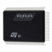
ST92F150CV1QB STMicroelectronics, ST92F150CV1QB Datasheet - Page 34

ST92F150CV1QB
Manufacturer Part Number
ST92F150CV1QB
Description
MCU 8BIT 128K FLASH 100PQFP
Manufacturer
STMicroelectronics
Series
ST9r
Datasheet
1.ST92F150CV1TB.pdf
(429 pages)
Specifications of ST92F150CV1QB
Core Processor
ST9
Core Size
8/16-Bit
Speed
24MHz
Connectivity
CAN, I²C, LIN, SCI, SPI
Peripherals
DMA, LVD, POR, PWM, WDT
Number Of I /o
77
Program Memory Size
128KB (128K x 8)
Program Memory Type
FLASH
Eeprom Size
1K x 8
Ram Size
4K x 8
Voltage - Supply (vcc/vdd)
4.5 V ~ 5.5 V
Data Converters
A/D 16x10b
Oscillator Type
Internal
Operating Temperature
-40°C ~ 105°C
Package / Case
100-QFP
Processor Series
ST92F15x
Core
ST9
Data Bus Width
8 bit, 16 bit
Data Ram Size
6 KB
Interface Type
CAN, I2C, SCI, SPI
Maximum Clock Frequency
24 MHz
Number Of Programmable I/os
80
Number Of Timers
5 x 16 bit
Operating Supply Voltage
4.5 V to 5.5 V
Maximum Operating Temperature
+ 105 C
Mounting Style
SMD/SMT
Development Tools By Supplier
ST92F150-EPB
Minimum Operating Temperature
- 40 C
On-chip Adc
16 bit x 10 bit
Lead Free Status / RoHS Status
Lead free / RoHS Compliant
Other names
497-4882
Available stocks
Company
Part Number
Manufacturer
Quantity
Price
Company:
Part Number:
ST92F150CV1QB
Manufacturer:
STMicroelectronics
Quantity:
10 000
- Current page: 34 of 429
- Download datasheet (8Mb)
ST92F124/F150/F250 - DEVICE ARCHITECTURE
2.3 SYSTEM REGISTERS
The System registers are listed in
are used to perform all the important system set-
tings. Their purpose is described in the following
pages. Refer to the chapter dealing with I/O for a
description of the PORT[5:0] Data registers.
Table 6. System Registers (Group E)
2.3.1 Central Interrupt Control Register
Please refer to the ”INTERRUPT” chapter for a de-
tailed description of the ST9 interrupt philosophy.
CENTRAL INTERRUPT CONTROL REGISTER
(CICR)
R230 - Read/Write
Register Group: E (System)
Reset Value: 1000 0111 (87h)
Bit 7 = GCEN: Global Counter Enable.
This bit is the Global Counter Enable of the Multi-
function Timers. The GCEN bit is ANDed with the
CE bit in the TCR Register (only in devices featur-
ing the MFT Multifunction Timer) in order to enable
the Timers when both bits are set. This bit is set af-
ter the Reset cycle.
34/429
9
GCE
R239 (EFh)
R238 (EEh)
R237 (EDh)
R236 (ECh)
R235 (EBh)
R234 (EAh)
R233 (E9h)
R232 (E8h)
R231 (E7h)
R230 (E6h)
R229 (E5h)
R228 (E4h)
R227 (E3h)
R226 (E2h)
R225 (E1h)
R224 (E0h)
N
7
TLIP
TLI
IEN
PAGE POINTER REGISTER
CENTRAL INT. CNTL REG
REGISTER POINTER 1
REGISTER POINTER 0
PORT5 DATA REG.
PORT4 DATA REG.
PORT3 DATA REG.
PORT2 DATA REG.
PORT1 DATA REG.
PORT0 DATA REG.
MODE REGISTER
FLAG REGISTER
IAM
SSPHR
USPHR
USPLR
SSPLR
CPL2 CPL1 CPL0
Table
6. They
0
Note: If an MFT is not included in the ST9 device,
then this bit has no effect.
Bit 6 = TLIP: Top Level Interrupt Pending.
This bit is set by hardware when a Top Level Inter-
rupt Request is recognized. This bit can also be
set by software to simulate a Top Level Interrupt
Request.
0: No Top Level Interrupt pending
1: Top Level Interrupt pending
Bit 5 = TLI: Top Level Interrupt bit.
0: Top Level Interrupt is acknowledged depending
1: Top Level Interrupt is acknowledged depending
Bit 4 = IEN: Interrupt Enable .
This bit is cleared by interrupt acknowledgement,
and set by interrupt return (iret). IEN is modified
implicitly by iret, ei and di instructions or by an
interrupt acknowledge cycle. It can also be explic-
itly written by the user, but only when no interrupt
is pending. Therefore, the user should execute a
di instruction (or guarantee by other means that
no interrupt request can arrive) before any write
operation to the CICR register.
0: Disable all interrupts except Top Level Interrupt.
1: Enable Interrupts
Bit 3 = IAM: Interrupt Arbitration Mode.
This bit is set and cleared by software to select the
arbitration mode.
0: Concurrent Mode
1: Nested Mode.
Bits 2:0 = CPL[2:0]: Current Priority Level.
These three bits record the priority level of the rou-
tine currently running (i.e. the Current Priority Lev-
el, CPL). The highest priority level is represented
by 000, and the lowest by 111. The CPL bits can
be set by hardware or software and provide the
reference according to which subsequent inter-
rupts are either left pending or are allowed to inter-
rupt the current interrupt service routine. When the
current interrupt is replaced by one of a higher pri-
ority, the current priority value is automatically
stored until required in the NICR register.
on the TLNM bit in the NICR Register.
on the IEN and TLNM bits in the NICR Register
(described in the Interrupt chapter).
Related parts for ST92F150CV1QB
Image
Part Number
Description
Manufacturer
Datasheet
Request
R

Part Number:
Description:
BOARD PROGRAM FOR ST92F150 MCU
Manufacturer:
STMicroelectronics
Datasheet:

Part Number:
Description:
BOARD EVALUATION FOR ST9 SERIES
Manufacturer:
STMicroelectronics
Datasheet:

Part Number:
Description:
BOARD EMULATOR FOR ST9 SERIES
Manufacturer:
STMicroelectronics
Datasheet:

Part Number:
Description:
MCU, MPU & DSP Development Tools ST9 Dedication Board
Manufacturer:
STMicroelectronics
Datasheet:

Part Number:
Description:
STMicroelectronics [RIPPLE-CARRY BINARY COUNTER/DIVIDERS]
Manufacturer:
STMicroelectronics
Datasheet:

Part Number:
Description:
STMicroelectronics [LIQUID-CRYSTAL DISPLAY DRIVERS]
Manufacturer:
STMicroelectronics
Datasheet:

Part Number:
Description:
BOARD EVAL FOR MEMS SENSORS
Manufacturer:
STMicroelectronics
Datasheet:

Part Number:
Description:
NPN TRANSISTOR POWER MODULE
Manufacturer:
STMicroelectronics
Datasheet:

Part Number:
Description:
TURBOSWITCH ULTRA-FAST HIGH VOLTAGE DIODE
Manufacturer:
STMicroelectronics
Datasheet:

Part Number:
Description:
Manufacturer:
STMicroelectronics
Datasheet:

Part Number:
Description:
DIODE / SCR MODULE
Manufacturer:
STMicroelectronics
Datasheet:

Part Number:
Description:
DIODE / SCR MODULE
Manufacturer:
STMicroelectronics
Datasheet:


