MCHC908JW32FAE Freescale Semiconductor, MCHC908JW32FAE Datasheet - Page 103
MCHC908JW32FAE
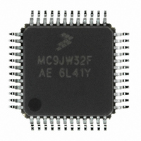
Manufacturer Part Number
MCHC908JW32FAE
Description
IC MCU 32K FLASH 8MHZ 48-LQFP
Manufacturer
Freescale Semiconductor
Series
HC08r
Datasheet
1.RD3152MMA7260Q.pdf
(232 pages)
Specifications of MCHC908JW32FAE
Core Processor
HC08
Core Size
8-Bit
Speed
8MHz
Connectivity
SPI, USB
Peripherals
LED, LVD, POR, PWM
Number Of I /o
29
Program Memory Size
32KB (32K x 8)
Program Memory Type
FLASH
Ram Size
1K x 8
Voltage - Supply (vcc/vdd)
3.5 V ~ 5.5 V
Oscillator Type
Internal
Operating Temperature
0°C ~ 70°C
Package / Case
48-LQFP
Controller Family/series
HC08
No. Of I/o's
48
Ram Memory Size
1KB
Cpu Speed
8MHz
No. Of Timers
1
Embedded Interface Type
SPI
Rohs Compliant
Yes
Processor Series
HC08JW
Core
HC08
Data Bus Width
8 bit
Data Ram Size
1 KB
Interface Type
SPI, USB
Number Of Programmable I/os
29
Number Of Timers
2
Maximum Operating Temperature
+ 70 C
Mounting Style
SMD/SMT
Development Tools By Supplier
FSICEBASE, DEMO908GZ60E, M68EML08GZE, KITUSBSPIDGLEVME, KITUSBSPIEVME, KIT33810EKEVME
Minimum Operating Temperature
0 C
Lead Free Status / RoHS Status
Lead free / RoHS Compliant
Eeprom Size
-
Data Converters
-
Lead Free Status / Rohs Status
Details
Available stocks
Company
Part Number
Manufacturer
Quantity
Price

Company:
Part Number:
MCHC908JW32FAE
Manufacturer:
Freescale Semiconductor
Quantity:
10 000
Part Number:
MCHC908JW32FAE
Manufacturer:
FREESCALE
Quantity:
20 000


7.5 ROM-Resident Routines
Five routines stored in the monitor ROM area (thus ROM-resident) are provided for FLASH memory
manipulation. They are intended to simplify FLASH program, erase and load operations.
shows a summary of the ROM-resident routines.
The routines are designed to be called as stand-alone subroutines in the user program or monitor mode.
The parameters that are passed to a routine are in the form of a contiguous data block, stored in RAM.
The index register (H:X) is loaded with the address of the first byte of the data block (acting as a pointer),
and the subroutine is called (JSR). Using the start address as a pointer, multiple data blocks can be used,
any area of RAM be used. A data block has the control and data bytes in a defined order, as shown in
Figure
During the software execution, it does not consume any dedicated RAM location, the run-time heap will
extend the system stack, all other RAM location will not be affected.
Freescale Semiconductor
7-8.
MON_PRGRNGE
MON_ERARNGE
Routine Name
PRGRNGE
ERARNGE
LDRNGE
ADDRESS AS POINTER
FILE_PTR
Figure 7-8. Data Block Format for ROM-Resident Routines
Table 7-10. Summary of ROM-Resident Routines
Program a range of locations
Erase a page or the entire array
Loads data from a range of locations
Program a range of locations in monitor
mode
Erase a page or the entire array in monitor
mode
ARRAY
DATA
MC68HC908JW32 Data Sheet, Rev. 6
$XXXX
Routine Description
START ADDRESS HIGH (ADDRH)
START ADDRESS LOW (ADDRL)
BUS SPEED (BUS_SPD)
DATA SIZE (DATASIZE)
R
DATA N
DATA 0
DATA 1
A
M
Address
$FE10
$FE13
$FA31
$FF24
$FF28
Call
BLOCK
DATA
ROM-Resident Routines
Stack Used
(bytes)
Table 7-10
16
10
10
18
12
103
Related parts for MCHC908JW32FAE
Image
Part Number
Description
Manufacturer
Datasheet
Request
R

Part Number:
Description:
Manufacturer:
Freescale Semiconductor, Inc
Datasheet:
Part Number:
Description:
Manufacturer:
Freescale Semiconductor, Inc
Datasheet:
Part Number:
Description:
Manufacturer:
Freescale Semiconductor, Inc
Datasheet:
Part Number:
Description:
Manufacturer:
Freescale Semiconductor, Inc
Datasheet:
Part Number:
Description:
Manufacturer:
Freescale Semiconductor, Inc
Datasheet:
Part Number:
Description:
Manufacturer:
Freescale Semiconductor, Inc
Datasheet:
Part Number:
Description:
Manufacturer:
Freescale Semiconductor, Inc
Datasheet:
Part Number:
Description:
Manufacturer:
Freescale Semiconductor, Inc
Datasheet:
Part Number:
Description:
Manufacturer:
Freescale Semiconductor, Inc
Datasheet:
Part Number:
Description:
Manufacturer:
Freescale Semiconductor, Inc
Datasheet:
Part Number:
Description:
Manufacturer:
Freescale Semiconductor, Inc
Datasheet:
Part Number:
Description:
Manufacturer:
Freescale Semiconductor, Inc
Datasheet:
Part Number:
Description:
Manufacturer:
Freescale Semiconductor, Inc
Datasheet:
Part Number:
Description:
Manufacturer:
Freescale Semiconductor, Inc
Datasheet:
Part Number:
Description:
Manufacturer:
Freescale Semiconductor, Inc
Datasheet: